...
Table 22-1 shows the relationship of ECC data spec, Parity data length and Protect software use byte.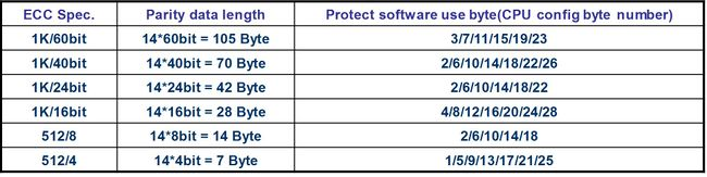
Table 22-1 ECC Data Format
"1KB/60bit" means the correct ability is 60bit within 1K byte date, "1KB/40bit" means the correct ability is 40bit within 1K byte date and so on.
The sum of the parity and SW protected data must be 4-byte align. The figure 22-2 is the example of ECC spec. as 1K/16b and software protected byte as 4 bytes case.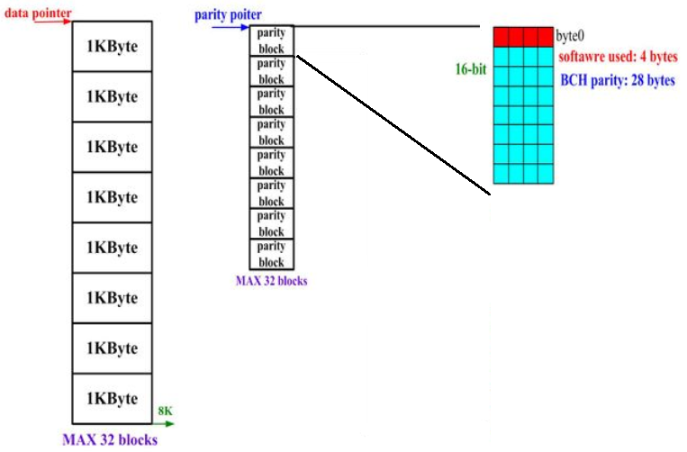
Figure 22-2 Software Protect Date Size
22.4 Auto BCH Enable
Set register Group 87.16 spi_bch bit4 to 1, it will enable auto BCH mode. Please refer to 22.6.2 registers description for more detail description.
22.5 BCH Interrupts
There are two kinds of interrupt.
Decode fail Interrupt is issued when bch can't fix data because too much error bits happens and Decode fail mask is true. Finish interrupt is issued when bch work finish and Finish mask is true.
Figure 22-3 shows the BCH interrupt tree.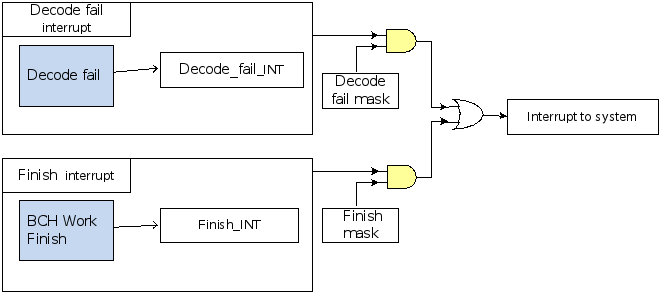
Figure 22-3 BCH Interrupt Tree
22.
...
6 Registers Map
22.
...
6.1 Registers Memory Map
BCH Group 0 BCH Controller
Address | Group No. | Register Name | Register Description |
0x9C101000 | G0.0 | configuration | bch control register |
0x9C101004 | G0.1 | data pointer | bch encode/decode data start address |
0x9C101008 | G0.2 | parity pointer | bch encode/decode parity start address |
0x9C10100C | G0.3 | Interrupt status | bch interrupt, write 1 clear |
0x9C101010 | G0.4 | Software clear flag | write 1 to reset bch |
0x9C101014 | G0.5 | Interrupt mask | bch interrupt mask control register |
0x9C101018 | G0.6 | Report status | bch report status |
0x9C10101C | G0.7 | Sector error report | report the Nth (N=0˜31) block has error bit or not |
0x9C101020 | G0.8 | Sector fail report | report the Nth (N=0˜31) block has to much error bits can't be fixed by decoder |
0x9C10102C | G0.11 | Control register | The controller register for ff&00 check and correction method |
RGST Table Group 87 SPI NAND Controller Registers
Address | Group No. | Register Name | Register Description |
| 0x9C002BC0 | G87.16 | spi_bch | SPI BCH configuration Register |
| Anchor | ||||
|---|---|---|---|---|
|
22.
...
6.2 Registers Description
BCH Group 0 BCH Controller
0.0 bch control register (configuration)
Address: 0x9C101000
Reset: 0x0
...
Field Name | Bit | Access | Description |
| Reserved | 31:3 | RO | |
| Last corr nonbufw | 2 | RW | Just the last sector use nonbufferable write 0: encode:all sectors use nonbufferable write for all the en- parity write; decode:all sectors use nonbufferable write for all correc- tion write(please set to '0' in decode mode); 1: encode:only last sector use nonbufferable write for en- parity(default) decode:not allowed |
| Reserved | 1:0 | RO |
RGST Table Group 87 SPI NAND Controller Registers
87.16 SPI BCH configuration Register (spi bch)
Address: 0x9C002BC0
Reset: 0x0000
Field Name | Bit | Access | Description |
| Reserved | 31:16 | RO | Default to be zero |
| BCH DATA LEN | 15:8 | RW | For bch data: 0x0: 0Byte parity data per BCH sector 0x1: 1Byte parity data per BCH sector ... 0xff: 255Byte parity data per BCH sector |
| Reserved | 7 | RO | Default to be zero |
| BCH DATA MODE | 6 | RW | BCH data mdoe select 0: 512Byte per BCH. 1: 1k Byte per BCH. |
| BCH ACC | 5 | RW | 32Byte or 16Byte align 0: 32Byte align. 1: 16Byte align. |
| AUTO BCH EN | 4 | RW | Auto BCH function enable Write 1 enable. It will encode data before the page program or decode data during page read. |
| SECTOR NUM | 3:0 | RW | Set the number N of block for BCH N= 0˜15(1˜16 blocks) |