...
A generalized function diagram of MailBox is shown in Figure 29-1.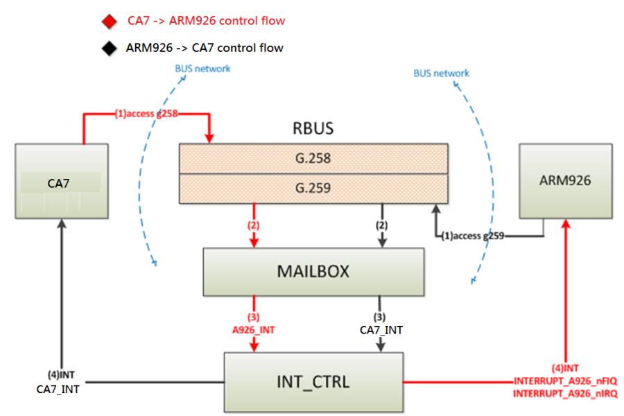
Figure 29-1 MailBox Functional Blocks
First Function Communication (Remote Function Call)
...
- CA7 writes the information to be exchanged into G258.4~31, but before writing, read G258.1[31:4] first, and confirm that the Register Status corresponding to each register is unlocked before it can be written. It indicate that register data has been read by ARM926, can be written to overwrite; but if it is forced to write register with register status of 1, the MailBox is processed by overwriting the previous data. This part should be noted in use. At the same time, Mailbox will pull the corresponding bit of the register to be written in G258.2[31:4] to 1 as the record of transaction overwrite flag.
- Finally, according to the first type of communication or the second type of communication to trigger the corresponding interrupt, notify ARM926 to read G258.4~31. The first type of communication before ARM926 read G258.4~23, read G258.1 at first. Only the register corresponding to Register Status is 1 can be read. The second type of communication will first read the corresponding bit of G258.1 according to the interrupt, to confirm that Register Status is 1, and then read from the corresponding register.
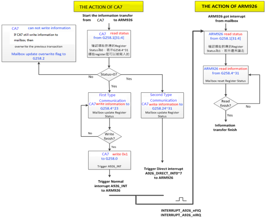
Figure 29-2 MailBox Firmware Architecture1
ARM926 read status before write information / CA7 read status before read information
- ARM926 writes the information to be exchanged into G259.4~31, but before writing, read G259.1[31:4] first, and confirm that the Register Status corresponding to each register is unlock. It indicates that register data has been read by CA7 and can be overwritten by the overlay. However, if the register with Register Status is 1 is forcibly written, the processing of MailBox is to overwrite the previous data. This part should be noted in use. At the same time, Mailbox will pull the corresponding bit of the register to be written in G259.2[31:4] to 1 as the record of transaction overwrite flag.
- Finally, trigger the corresponding interrupt according to the first type of communication or the second type of communication, and notify CA7 to read G259.4~31. The first type of communication should be before CA7 read G259.4~23, read G259.1 at first. Only read the register corresponding to Register Status is 1. The second type of communication will first read the corresponding bit of G259.1 according to the interrupt, to confirm the Register Status is 1, then read from the corresponding register.
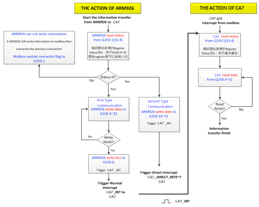
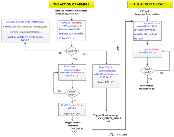
Figure 29-3 MailBox Firmware Architecture2
...
Address | Group No. | Register Name | Register Description | ||
0x9C008180 | G259.0 | Mbox_cpua_int_trigger | Trigger CPUA_INT | ||
0x9C008184 | G259.1 | Mbox1_writelock_flag | Monitor the writelock status of mailbox1 | ||
0x9C008188 | G259.2 | Mbox1_overwrite_flag | Monitor the overwrite status of mailbox1 | ||
0x9C00818C | G259.3 | RESERVED | |||
0x9C008190 | G259.4 | Mbox1_normal_trans[0] | Normal data transfer from CPUB to CPUA | ||
~~ | ~~ | ~~ | ~~ | ||
0x9C0081DC | G259.23 | Mbox1_normal_trans[19] | Normal data transfer from CPUB to CPUA | ||
0x9C0081E0 | G259.24 | Mbox1_direct_trans[0] | Direct data transfer from CPUB to CPUA | ||
~~ | ~~ | ~~ | _GoBack | _GoBack~~ | |
0x9C0081FC | G259.31 | Mbox1_direct_trans[7] | Direct data transfer from CPUB to CPUA |
| Anchor | ||||
|---|---|---|---|---|
|
29.4.2 Registers Description
...