30.1 Introduction
...
- MST_CORE: Receive or transmit data from or to SPI_SLAVE
- DMA_CTRL_W: Receive DATA from MST_CORE and produce WDATA_REQ with transmit 4-byte data to DMA_LINK_W
- DMA_CTRL_R: Transmit DATA to MST_CORE and produce RDATA_REQ with receive 4-byte data from DMA_LINK_R
- DMA_LINK_R/W: Communicate with DMA_CTRL via proprietary System Bus (SBUS) protocol
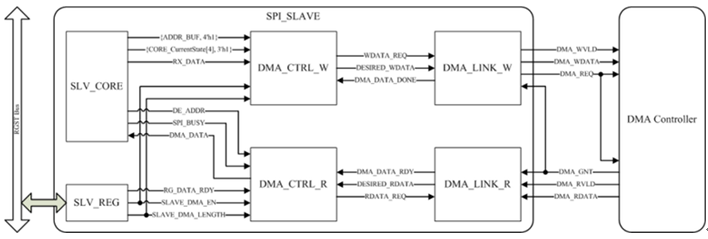
Figure 30-4 SPI Slave DMA Function Block
...
All SPIs' registers have the same offset (address - base address) in corresponding SPI register group. Only SPI0 Master and Slave registers are described in following register description, for other SPIs (SPI1, 2, 3) please refer to SPI0 description for more detail.
30.15.2 Registers Description
| Anchor | ||||
|---|---|---|---|---|
|
SPI Register Description
RGST Table Group 91 SPI MASTER 0
...
91.0 Transmit register1 (tx data addr)
Address: 0x9C002D80
Reset: 0x0000 0000
Field Name | Bit | Access | Description |
Reserve | 31:20 | RO | Reserved |
ADDR | 19:0 | RW | Address for SPI master to transmit in write/ read action |
...
91.2 Transmit register3 (tx data7 6 5 4)
Address: 0x9C002D88
Reset: 0x0000 0000
Field Name | Bit | Access | Description |
TX DATA 5 | 15:8 | RW | Byte5 data for SPI master to transmit in write action |
TX DATA 4 | 7:0 | RW | Byte4 data for SPI master to transmit in write action |
...
91.9 Receive register1 (rx data3 2 1 0)
Address: 0x9C002DA4
Reset: 0x0000 0000
Field Name | Bit | Access | Description |
RX DATA 3 | 31:24 | RO | Byte3 data that SPI master receive in read action |
RX DATA 2 | 23:16 | RO | Byte2 data that SPI master receive in read action |
RX DATA 1 | 15:8 | RO | Byte1 data that SPI master receive in read action |
RX DATA 0 | 7:0 | RO | Byte0 data that SPI master receive in read action |
...
91.10 Receive register2 (rx data7 6 5 4)
Address: 0x9C002DA8
Reset: 0x0000 0000
Field Name | Bit | Access | Description |
RX DATA 7 | 31:24 | RO | Byte7 data that SPI master receive in read action |
RX DATA 6 | 23:16 | RO | Byte6 data that SPI master receive in read action |
RX DATA 5 | 15:8 | RO | Byte5 data that SPI master receive in read action |
RX DATA 4 | 7:0 | RO | Byte4 data that SPI master receive in read action |
...
Field Name | Bit | Access | Description |
REG_TOTAL_LENGTH_FD | 31:24 | RW | Total length for full duplex |
REG_TX_LENGTH_FD | 23:16 | RW | TX length for full duplex max 255 byte,less than total length |
REG_RX_CNT | 15:12 | RO | RX FIFO CNT for full duplex data byte in rx fifo, |
REG_TX_CNT | 11:8 | RO | TX FIFO CNT for full duplex data byte in tx fifo, |
REG_SPI_BUSY_FD | 7 | RO | SPI_BUSY for full duplex 0: busy |
REG_FINISH_FLAG | 6 | WO | FINISH_FLAG for full duplex |
REG_RX_FUL_FLAG | 5 | RO | RX_FIFO_FUL_FLAG for full duplex |
REG_RX_EMP_FLAG | 4 | RO | RX_FIFO_EMP_FLAG for full duplex |
REG_TX_FUL_FLAG | 3 | RO | TX_FIFO_FUL_FLAG for full duplex |
REG_TX_EMP_FLAG | 2 | RO | TX_FIFO_EMP_FLAG for full duplex |
REG_MASTER_SW_RST | 1 | RO | SW RST for full duplex |
REG_SPI_START_FD | 0 | RO | SPI START for full duplex |
...
Field Name | Bit | Access | Description |
REG_SPI_CLK_CNT_FD | 31:16 | RW | Ratio between SPI clk and sysclk |
REG_FINISH_MASK | 15 | RW | FINISH_MASK for full duplex |
REG_RX_FUL_MASK | 14 | RW | RX_FIFO_FUL_MASK for full duplex |
REG_RX_EMP_MASK | 13 | RW | RX_FIFO_EMP_MASK for full duplex |
REG_TX_FUL_MASK | 12 | RW | TX_FIFO_FUL_MASK for full duplex |
REG_TX_EMP_MASK | 11 | RW | TX_FIFO_EMP_MASK for full duplex |
REG_WRITE_BYTE | 10:9 | RW | WRITE_BYTE for full duplex |
REG_READ_BYTE | 8:7 | RW | READ_BYTE for full duplex |
REG_HALF_FULL_SEL | 6 | RO | HALF_FULL_SEL for full duplex 0: half duplex mode |
REG_EN_POR_FD | 5 | RW | EN POLARITY for full duplex 0: cs low active |
REG_LSB_SEL_FD | 4 | RW | LSB SELECT for full duplex 0: msb |
REG_DELAY_FD | 3 | RW | DEALY ENABLE IN RX for full duplex |
REG_CPHA_W_FD | 2 | RW | CPHA_W TX for full duplex 0: first edge launch |
REG_CPHA_R_FD | 1 | RW | CPHA_R RX for full duplex 0: first edge capture |
REG_CPOL_FD | 0 | RW | CPOL for full duplex 0:- clk low when idle |
91.17 SPI master control and clock select register (spi ctrl clk sel)
Address: 0x9C002DC4
Reset: 0x0000 0000
Field Name | Bit | Access | Description |
R DLY | 31:30 | RW | Additional delay in read action 0x0: No delay(default) |
SPI CLOCK SEL | 29:16 | RW | Ratio between SPI clk and sysclk1/(2*(CLK SEL+1)) |
Reserve | 15:9 | RW | Reserved |
ADDR BIT NUM | 8:7 | RW | Transfer address bit number 0x0: 12-bit |
WRITE SAMPLING EDGE | 6 | RW | SPI TX edge 0: Rising edge of SPI clk(default) |
READ SAMPLING EDGE | 5 | RW | SPI RX edge 0: Rising edge of SPI clk(default) |
EN POLARITY | 4 | RW | SPI CS polarity 0: Low active(default) |
READ POLARITY | 3 | RW | Read/Write bit polarity 0: High read(default) |
RW POSITION | 2 | RW | Read/Write bit position 0: Addr[0] is R/W bit(default) |
SB SELECT | 1 | RW | LSB enable in SPI transmission 0: Begin at bit0(default) |
SPISTART | 1 | WO | SPI transmission start 1: SPI master begin write/ read action |
91.18 SPI transmission byte No. register (byte no)
Address: 0x9C002DC8
Reset: 0x0000 0000
Field Name | Bit | Access | Description |
Reserve | 31:5 | RO | Reserved |
BYTE NO | 4:0 | RW | No. of bytes in SPI transmission Support from 1-byte to 16-byte |
...
Field Name | Bit | Access | Description |
Reserve | 31:10 | RO | RESERVED |
PI BUSY FLAG | 9 | RO | Indicator of BUSY signal from TI2046 chip |
PI BUSY EN | 8 | RO | Support TI2046 BUSY signal Return data is valid when busy signal is low after SPI MASTER issues command. |
MASTER INT STATUS | 7 | RO | Master interrupt to RISC |
MASTER INT CLR | 6 | RW | Master INT clear 1: Clear SPI master interrupt |
REG INT EDGE | 5 | RW | Define incoming SPI interrupt trigger polarity 0: low level or falling edge interrupt |
REG INT TYPE | 4 | RW | Define incoming SPI interrupt trigger type 0: level interrupt(default) |
REG INT BYPASS | 3 | RW | SPI master INT bypass 0: SPI master INT comes from SPI master module(default) |
REG INT TIMEOUT | 2 | RW | SPI master INT timeout function SPI master module will launch SPI master INT again when CPU has served INT but the incoming SPI interrupt is still in active state. |
RW PHASE | 1 | RO | Indicator of SPI write/ read action 0: read(default) |
REG SPI BUSY | 0 | RO | Indicator of SPI master operation status 0: SPI master is not in operation(default) |
91.20 SPI master DMA control register (master dma ctrl)
Address: 0x9C002DD0
Reset: 0x0000 0000
Field Name | Bit | Access | Description |
Reserve | 31:9 | RO | RESERVED |
DMA W INT STATUS | 8 | RO | DMA Write interrupt status Whether DMA transmission is finished or not. |
DMA W INT CLR | 7 | RW | DMA Write interrupt clear 1: Clear DMA write interrupt |
DMA RW SEL | 6 | RW | DMA read/write select 0: DMA write to DRAM(default) |
DMA BANK | 5 | RW | DRAM bank select 0x0: Bank A(default) |
MASTER DMA BP WBE | 4 | RWRW | SBUS write-byte enable select 0: With write-byte-enable(default) |
MASTER DMA BURST | 3:2 | SBUS command select 0x0: 4 bytes command(default) | |
MASTER MASTER SW RST | 1 | RW | SPI master software reset 0: Disable(default) |
MASTER DMA EN | 0 | RW | DMA function select 0: Disable(default) |
91.21 SPI master DMA length register (master dma length)
Address: 0x9C002DD4
Reset: 0x0000 0000
Field Name | Bit | Access | Description |
Reserve | 31:18 | RO | RESERVED |
MASTER DMA LENGTH | 17:0 | RW | Total data length in DMA transmission (unit:byte) |
91.22 SPI master DMA address register (master dma addr)
Address: 0x9C002DD8
Reset: 0x0000 0000
Field Name | Bit | Access | Description |
MASTER DMA ADDR | 31:0 | RW | Start address in DRAM to store data (unit:byte) |
...
91.24 SPI master DMA address status register (dma addr status)
Address: 0x9C002DE0
Reset: 0x0000 0000
Field Name | Bit | Access | Description |
DMA ADDR STATUS | 31:0 | RO | DMA address status Return address which DMA access |
...
91.26 Uart DMA control register (uart dma ctrl)
Address:0x9C002DE8
Reset: 0x0000 0000
Field Name | Bit | Access | Description |
Reserve | 31:3 | RO | RESERVED |
UART SW RST | 2 | RW | Software reset when SPI in UART DMA mode |
UART DMA START | 1 | W1C | DMA transmission start signal from UART 1: DMA transmission start ; it will return to 0 automatically. |
UART DMA EN | 0 | RW | DMA function select from UART 0: Disable(default) |
91.28 Reserved (reserved)
Address: 0x9C002DF0
Reset: 0x0000 0000
Field Name | Bit | Access | Description |
Reserve | 31:0 | RO | Reserved for Internal usage purpose |
...
91.29 Reserved (Reserved)
Address: 0x9C002DF4
Reset: 0x0000 0000
Field Name | Bit | Access | Description |
Reserve | 31:0 | RO | Reserved for Internal usage purpose |
...
91.30 SPI extra cycle control register (spi extra cycle ctrl)
Address: 0x9C002DF8
Reset: 0x0000 0000
Field Name | Bit | Access | Description |
Reserve | 31:4 | RO | RESERVED |
SPI EXTRA CYCLE | 3:2 | RW | Choose the number of SPI extra cycle. These settings take effect ONLY when SPI EXTRA CYCLE EN=1'b1 0x0: Add extra 1 SPI cycle(default) |
SPI EN CUT | 1 | RW | SPI EN output interval select This setting takes effect ONLY when SPI EXTRA CYCLE EN=1'b1 0: SPI EN output interval will be SPI read plus SPI extra cycle.(default) |
SPI EXTRA CYCLE EN | 0 | RW | Enable SPI extra cycle to fix path delay in SPI read process 0: Disable(default) |
91.31DMA data ready register (dma data ready)
Address: 0x9C002DFC
Reset: 0x0000 0000
Field Name | Bit | Access | Description |
Reserve | 31:1 | RO | RESERVED |
MST DMA DATA RDY | 0 | RO | DMA Read data prefetch ready |
...
92.0 SPI slave transmit data register1 (tx data2 1 0)
Address: 0x9C002E00
Reset: 0x0000 0000
Field Name | Bit | Access | Description |
RESERVED | 31:24 | RO | RESERVED |
TX DATA 2 | 23:16 | RW | Byte2 data for SPI slave to transmit in read action |
TX DATA 1 | 15:8 | RW | Byte1 data for SPI slave to transmit in read action |
TX DATA 0 | 7:0 | RW | Byte0 data for SPI slave to transmit in read action |
92.1SPI slave transmit data register2 (tx data6 5 4 3)
Address: 0x9C002E04
Reset: 0x0000 0000
Field Name | Bit | Access | Description |
TX DATA 6 | 31:24 | RW | Byte6 data for SPI slave to transmit in read action |
TX DATA 5 | 23:16 | RW | Byte5 data for SPI slave to transmit in read action |
TX DATA 4 | 15:8 | RW | Byte4 data for SPI slave to transmit in read action |
TX DATA 3 | 7:0 | RW | Byte3 data for SPI slave to transmit in read action |
...
92.4 SPI slave transmit data register5 (tx data15)
Address: 0x9C002E10
Reset: 0x0000 0000
Field Name | Bit | Access | Description |
RESERVED | 31:8 | RO | RESERVED |
TX DATA 15 | 7:0 | RW | Byte15 data for SPI slave to transmit in read action |
...
92.9 SPI slave receive data register1 (rx data3 2 1 0)
Address: 0x9C002E24
Reset: 0x0000 0000
Field Name | Bit | Access | Description |
RX DATA 3 | 31:24 | RO | Byte3 data that SPI slave receive in write action |
RX DATA 2 | 23:16 | RO | Byte2 data that SPI slave receive in write action |
RX DATA 1 | 15:8 | RO | Byte1 data that SPI slave receive in write action |
RX DATA 0 | 7:0 | RO | Byte0 data that SPI slave receive in write action |
...
92.10 SPI slave receive data register2 (rx data7 6 5 4)
Address: 0x9C002E28
Reset: 0x0000 0000
Field Name | Bit | Access | Description |
RX DATA 7 | 31:24 | RO | Byte7 data that SPI slave receive in write action |
RX DATA 6 | 23:16 | RO | Byte6 data that SPI slave receive in write action |
RX DATA 5 | 15:8 | RO | Byte5 data that SPI slave receive in write action |
RX DATA 4 | 7:0 | RO | Byte4 data that SPI slave receive in write action |
...
92.17 SPI slave interrupt register (risc int data rdy)
Address: 0x9C002E44
Reset: 0x0000 0000
Field Name | Bit | Access | Description |
RESERVED | 31:10 | RO | RESERVED |
SPI SLAVE INT | 9 | RO | SPI Slave Interrupt Register SPI slave will launch INT to CPU when SPI transmission is finished no matter write or read action. |
SLAVE INT CLR | 8 | RW | SPI slave INT clear 1: Clear SPI slave interruptit will return to 0 automatically when interrupt is low. |
RESERVED | 7:1 | RO | RESERVED |
SLAVE DATA RDY | 0 | RW | SPI slave data ready signal 1: SPI slave data is ready and launch INT to SPI master. It will return to 0 automatically. |
...
92.18 SPI slave DMA control register (slave dma ctrl)
Address: 0x9C002E48
Reset: 0x0000 0000
Field Name | Bit | Access | Description |
RESERVED | 31:7 | RO | RESERVED |
SLAVE DMA RW SEL | 6 | RW | SLAVE DMA read/write select 0: DMA write to DRAM(default) |
SLAVE DMA BANK | 5 | RW | DRAM bank select 0: Bank A(default) |
SLAVE DMA BP WBE | 4 | RW | SBUS write-byte enable select 0: With write-byte-enable(default) |
SLAVE DMA BURST | 3:2 | RW | SBUS command select 0x0: 4 bytes command(default) |
SLAVE SLAVE SW RST | 1 | RW | SPI slave software reset 0: Disable(default) |
SLAVE DMA EN | 0 | RW | DMA function select 0: Disable(default) |
92.19 SPI slave DMA length register (slave dma length)
...
Field Name | Bit | Access | Description |
RESERVED | 31:18 | RO | RESERVED |
SLAVE DMA LENGTH | 17:0 | RW | Total data length in DMA transmission (unit:byte) |
92.20 SPI slave DMA address register (slave dma addr)
Address:0x9C002E50
Reset: 0x0000 0000
Field Name | Bit | Access | Description |
SLAVE DMA ADDR | 31:0 | RW | Slave Mode DMA Start Address |
...
Field Name | Bit | Access | Description |
RESERVED | 31:15 | RO | RESERVED |
SLAVE ADDR INFO | 14:8 | RO | Address info inside SPI slave module |
RESERVED | 7:2 | RO | RESERVED |
SLAVE RWPHASE | 1 | RO | Indicator of SPI write/read action 0: read (default) |
SLAVE BUSY | 0 | RO | Indicator of SPI slave operation status 0: SPI slave is not in operation (default) |
92.24 Reserved (Reserved)
Address: 0x9C002E60
Reset: 0x0000 0000
Field Name | Bit | Access | Description |
RESERVED | 31:0 | RO | RESERVED |
...