16. SDRAM
16.1 Introduction
The SP7021 utilizes system in package (SIP) technology to provide an internal buffer SDARM within the package. The SP7021 supports 1Gb and 4Gb of internal SDRAMs. The SDRAM is DDR3 (Double Data Rate 3) 1066max type and uses a 16-bit data interface. 16-bit and 8-bit data interfaces are both supported. It supports DFI2.1 to DRAM controller with DFI and PHY clock ratio is 1:2 and 1:1. The DRAM memory map area locates at address 0x00000000~0x1FFFFFFF which have 512MB size.
16.2 Function Diagram
The SP7021 DRAM controller used uMCTL2 IP and the function diagram is shown in Figure 16-1. The uMCTL2 receives transactions from the SoC core. These transactions are queued internally and scheduled for access in order to the SDRAM while satisfying the SDRAM protocol timing requirements, transaction priorities, and dependencies between the transactions. The uMCTL2 issues commands on the DFI interface to the PHY module, which launches and captures data to and from the SDRAM.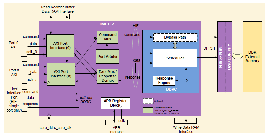
Figure 16-1 DRAM Controller Functional Blocks
The uMCTL2 contains the following main architectural components
- The AXI Port Interface (XPI) block: This block provides the interface to the application ports. It provides bus protocol handling, data buffering and reordering for read data, data bus size conversion (upsizing or downsizing), and memory burst address alignment. Read data is stored in a SRAM, read re-order buffer and returned in order, to the AXI ports. The SRAM may be instantiated as embedded memory external to the uMCTL2 or implemented as flops within the uMCTL2.
- The Port Arbiter (PA) block: This block provides latency sensitive, priority based arbitration between the addresses issued by the XPIs (by the ports).
- The DDR Controller (DDRC) block: This block contains a logical CAM (Content Addressable Memory), which can be synthesized using standard cells. This holds information on the commands, which is used by the scheduling algorithms to optimally schedule commands to be sent to the PHY, based on priority, bank/rank status and DDR timing constraints. A bypass path is also provided (optionally).
- The APB Register Block: This block contains the software accessible registers.
The DDR PHY is designed to connect the DRAM (dynamic random access memory) controller and DDR (Double Data Rate) 3 DRAM device. It contains the DDR PHY Control Unit (DPCU) and the Analog part (APHY). The interface between DRAM controller and the DDR PHY is compliant with DFI 2.1(DDR PHY Interface) protocol. The DDR PHY includes APHY initialization, data training, DRAM initialization, hardware VT compensation, and hardware auto timing update functionalities, as is used to enhance the whole DRAM system and to become robust and reliable. Figure 16-2 shows a DDR PHY block diagram.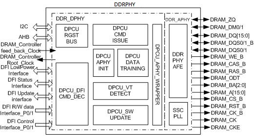
Figure 16-2 DDR PHY Block Diagram
- DPCU_DFI_CMD_DEC: This module is used to decode DFI commands from DRAM controller for DRAM device.
- DPCU_APHY_INIT: DPCU_APHY_INIT controls the initial flow for analog part (APHY).
- DPCU_DATA_TRAINING: This is the crucial part of DDRPHY, and it is used to do data training, which is the process to acquire optimal timing between signals for DRAM write/read transactions.
- DPCU_CMD_ISSUE: This module works like a lite DRAM controller. It can generate DRAM commands and the timing between those commands is guaranteed to meet DRAM specification.
- DPCU_VT_DETECT: Since process, voltage and temperature can deviate the delay of delay cells, this module is used to compensate those non-ideal effects.
- DPCU_SW_UPDATE: If the system need to change some settings of delay cells by software, this module can update those settings in a suitable period.
- DPCU_RGST_BUS: The communication interface between CPU and DDRPHY.
- DPCU_APHY_WRAPPER: The interface between DPCU and APHY.
- DDR_APHY: Analog part of DDRPHY which provide the interface with DDR device.
Note: There have critical timing between CPU and SDRAM, we don't prefer user to tune that. If you have special request in SDRAM support, please contact edwin.chiu@sunplus.com.