27. FPGA Interface
27.1 Introduction
SP7021 can connect to external FPGA thru many different ways, like thru I2C, GPIO or SDIO. For higher bandwidth application, SP7021 supports high performance interface to connect to external FPGA. The FPGA interface implements by FBIO module which provides a special interface for SP7021 and FPGA. This document provides a guide for customer to connect FPGA with the SP7021 peripheral pins and also describes how to access FPGA module through this interface. It provides a convenience method to communicate with FPGA and more efficiency method to verify the FPGA function. Compare to marketing FPGA verification tools, It also save much cost.
27.2 Function Diagram
Figure 27-1 shows an example of SP7021 connect to FPGA through FBIO interface.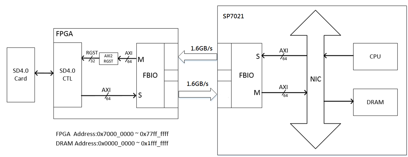
Figure 27-1 Example Of FBIO Connection
For example, the original SP7021 does not support the SD4.0 function. To use the SD4.0 card, we can extend the SD4.0 interface on the FPGA and use the SD card. Similarly, any IP without resources in SP7021 can be extended.
As shown in the figure, the address assigned by the IC to the FPGA is 0x7000_0000~0x77ff_ffff, and the register mapping of the SD4.0 CTL is at this address. After the CPU sends the command to the FPGA through FBIO, the 64-bit AXI bus is converted to the 32-bit RGST bus, and the registers in SD4.0 are configured to control the read and write transmission of the SD card.
Similarly, the FPGA can also access the IP in the IC through the corresponding address. Taking DRAM as an example, the address assigned by the IC to the DRAM is 0x0000_0000~0x1fff_ffff. The SD4.0 CTL on the FPGA can transfer addresses and instructions to the NIC via FBIO, then address the DRAM and read and write to the DRAM.
When the hardware platform of the IC and FPGA is set up, the IC accesses the FPGA and accesses the IP address corresponding to the NIC. So for the CPU, accessing the FPGA is the same as accessing other IPs such as SPI and USB. FBIO offers the opportunity to expand or quickly develop IP through FPGAs.
27.3 Enable FPGA Interface
FBIO function mode can be enabled while G1.1 register bit12 set to 1, GPIO_P0_02 ~ GPIO_P5_02 pins will be set to FBIO function for FPGA usage. But the priority is GPIO function > Multiplex Peripheral Pin > FBIO Function.While use FBIO function, do not set GPIO function and Multiplex Peripheral Pin within GPIO_P0_02 ~ GPIO_P5_02 pins. Please refer to chapter6 PIN MULTIPLEX FUNCTION for more detail description.
PS. SUNPLUS will provide FBIO module protocol for the customers who want to design FPGA connected with SP7021.
27.4 FBIO Source code Ref