28. Audio
28.1 Introduction
The 【AUD module】is an abbreviation of Audio. This module manages all of the audio playback. It contains the standard I2S and S/PDIF interface (Encode/Decode), signals record from ADC, and multi-channel mix. It supports up to 192KHz sample rate. When the audio data has been decoded by DSP and saved in DRAM, AUD module will fetch the data from DRAM and encode it with I2S or SPDIF protocol. It also can decode the I2s or SPDIF signal and save the data in DRAM for further usage.
28.2 Function Diagram
The input path is shown as figure 28-1 and the output path is shown as figure 28-2. The hardware block diagram is shown as figure 28-3..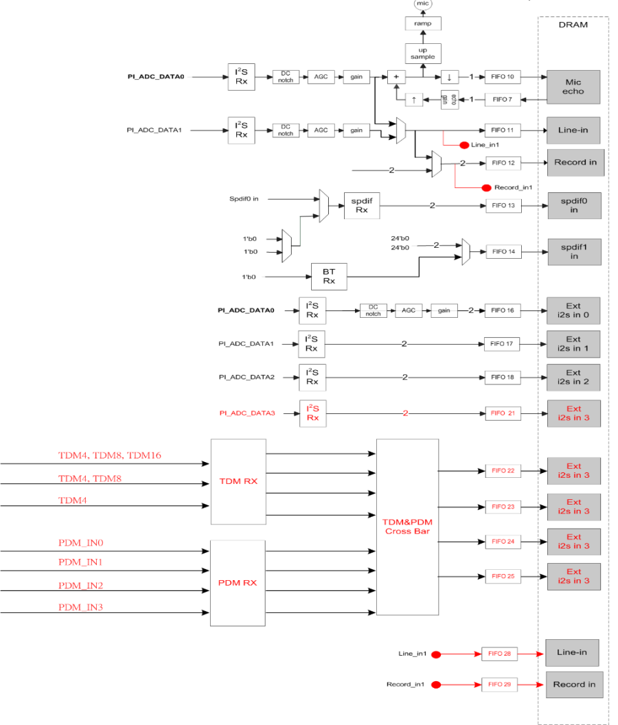
Figure 28-1 AUD Intput Functional Blocks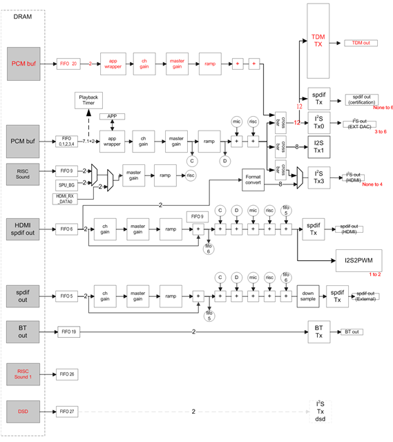
Figure 28-2 AUD Output Functional Blocks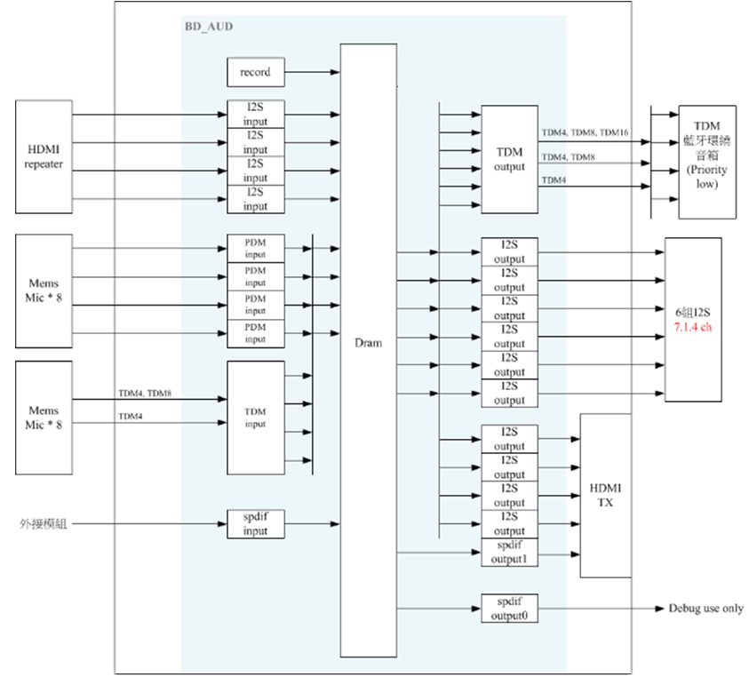
Figure 28-3 AUD Hardware Functional Blocks
The I2S output up to 6 stereo channels and input up to 4 stereo channels.
The SPDIF interface support one output and one input.
The TDM/PDM interface support up to 8 channel microphone array.
28.3 Pin assignment
GPIO_P1_00 ~ GPIO_P1_06 pins will be set to I2S audio IN function while G1.1 register bit15 set to 1. (Please refer to table 28-1)
GPIO_P2_05 ~ GPIO_P3_05 pins will be set to I2S audio OUT function while G1.2 register bit0 set to 1. (Please refer to table 28-1)
GPIO_P2_04 pin will be set to SPDIF IN function while G1.2 register bit2 set to 1. (Please refer to table 28-2)
GPIO_P2_04 pin will be set to SPDIF OUT function while G1.2 register bit3 set to 1. (Please refer to table 28-2)
GPIO_P2_05 ~ GPIO_P3_02 pins will be set to TDM TX function while G1.2 register bit4 set to 1. (Please refer to table 28-3)
GPIO_P1_07 ~ GPIO_P2_02 pins will be set to TDM RX function while G1.2 register bit5 set to 1. (Please refer to table 28-3)
GPIO_P1_07 ~ GPIO_P2_03 pins will be set to PDM RX function while G1.2 register bit6 set to 1. (Please refer to table 28-4)
GPIO_P3_07 ~ GPIO_P4_04 pins will be set to PCM function while G1.2 register bit7 set to 1. (Please refer to table 28-5)
While use audio function, do not set GPIO function and Multiplex Peripheral Pin within GPIO_P1_00 ~ GPIO_P4_04 pins.
Please also careful that some pins have multiplex functions, don't enable them at the same time.
Pin Name | I2S audio IN signals | I2S audio OUT signals |
GPIO_P1_00 | CLKGENA_EXT_ADC_XCK_O | |
GPIO_P1_01 | ADC_BCK | |
GPIO_P1_02 | ADC_LRCK | |
GPIO_P1_03 | ADC_DATA0 | |
GPIO_P1_04 | ADC_DATA1 | |
GPIO_P1_05 | ADC_DATA2 | |
GPIO_P1_06 | ADC_DATA3 | |
GPIO_P2_05 | CLKGENA_EXT_DAT_XCK | |
GPIO_P2_06 | AU_BCK | |
GPIO_P2_07 | AU_LRCK | |
GPIO_P3_00 | AU_DATA0 | |
GPIO_P3_01 | AU_DATA1 | |
GPIO_P3_02 | AU_DATA2 | |
GPIO_P3_03 | AU_DATA3 | |
GPIO_P3_04 | AU_DATA4 | |
GPIO_P3_05 | AU_DATA5 |
Table 28-1 I2C audio pin define
Pin Name | SPDIF IN signals | SPDIF OUT signals |
GPIO_P2_04 | AUD_IEC0_RX | |
GPIO_P3_06 | AUD_IEC0_TX |
Table 28-2 SPDIF pin define
Pin Name | TDM TX signals | TDM RX signals |
GPIO_P2_05 | CLKGENA_TDMTX_XCK_O | |
GPIO_P2_06 | TDMTX_BCK | |
GPIO_P2_07 | TDMTX_SYNC | |
GPIO_P3_00 | TDMTX_DATA4 | |
GPIO_P3_01 | TDMTX_DATA8 | |
GPIO_P3_02 | TDMTX_DATA16 | |
GPIO_P1_07 | TDMRX_BCK | |
GPIO_P2_00 | TDMRX_SYNC | |
GPIO_P2_01 | TDMRX_DATA4 | |
GPIO_P2_02 | TDMRX_DATA8 |
Table 28-3 TDM pin define
Pin Name | PDM RX signals |
GPIO_P1_07 | PDMRX_BCK |
GPIO_P2_00 | PDMRX_DATA0 |
GPIO_P2_01 | PDMRX_DATA1 |
GPIO_P2_02 | PDMRX_DATA2 |
GPIO_P2_03 | PDMRX_DATA3 |
Table 28-4 PDM pin define
Pin Name | PCM signals |
GPIO_P3_07 | PCM_IEC_TX0 |
GPIO_P4_00 | PCM_IEC_TX1 |
GPIO_P4_01 | PCM_IEC_TX2 |
GPIO_P4_02 | PCM_IEC_TX3 |
GPIO_P4_03 | PCM_IEC_TX4 |
GPIO_P4_04 | PCM_IEC_TX5 |
Table 28-5 PCM pin define
28.4 Registers Map
28.4.1 Registers Memory Map
Address | Group No. | Register Name | Description |
0x9C001E00 | G60.0 | audif_ctrl | AUD Interface Control |
0x9C001E04 | G60.1 | aud_enable | Audio FIFO Request Enable |
0x9C001E08 | G60.2 | pcm_cfg | Audio PCM (I2S) Format Configuration |
0x9C001E0C | G60.3 | i2s_mute_flag_ctrl | Mute Flag of I2S TX Module |
0x9C001E10 | G60.4 | ext_adc_cfg | External ADC (I2S) Format Configuration |
0x9C001E14 | G60.5 | int_dac_ctrl0 | Internal DAC Control 0 (ACODEC_CFG0) |
0x9C001E18 | G60.6 | int_adc_ctrl | Internal ADC Config |
0x9C001E1C | G60.7 | adc_in_path_switch | ADC Input Path Switch |
0x9C001E20 | G60.8 | int_adc_dac_cfg | Internal ADC and DAC (I2S) Format Configuration |
0x9C001E24 | G60.9 | reserved | Reserved |
0x9C001E28 | G60.10 | iec_cfg | S/PDIF Configuration |
0x9C001E2C | G60.11 | iec0_valid_out | Valid Bit for S/PDIF TX0 |
0x9C001E30 | G60.12 | iec0_par0_out | Channel Status of S/PDIF TX0 |
0x9C001E34 | G60.13 | iec0_par1_out | Channel Status of S/PDIF TX0 |
0x9C001E38 | G60.14 | iec1_valid_out | Valid Bit for S/PDIF TX1 |
0x9C001E3C | G60.15 | iec1_par0_out | Channel Status of S/PDIF TX1 |
0x9C001E40 | G60.16 | iec1_par1_out | Channel Status of S/PDIF TX1 |
0x9C001E44 | G60.17 | iec0_rx_debug_info | Debug Information of S/PDIF RX0 |
0x9C001E48 | G60.18 | iec0_valid_in | Valid Bit of S/PDIF RX0 |
0x9C001E4C | G60.19 | iec0_par0_in | Channel Status of S/PDIF RX0 |
0x9C001E50 | G60.20 | iec0_par1_in | Channel Status of S/PDIF RX0 |
0x9C001E54 | G60.21 | iec1_rx_debug_info | Debug Information of S/PDIF RX1 |
0x9C001E58 | G60.22 | iec1_valid_in | Valid Bit of S/PDIF RX1 |
0x9C001E5C | G60.23 | iec1_par0_in | Channel Status of S/PDIF RX1 |
0x9C001E60 | G60.24 | iec1_par1_in | Channel Status of S/PDIF RX1 |
0x9C001E64 | G60.25 | iec2_rx_debug_info | Debug Information of S/PDIF RX2 |
0x9C001E68 | G60.26 | iec2_valid_in | Valid Bit of S/PDIF RX2 |
0x9C001E6C | G60.27 | iec2_par0_in | Channel Status of S/PDIF RX2 |
0x9C001E70 | G60.28 | iec2_par1_in | Channel Status of S/PDIF RX2 |
0x9C001E74 | G60.29 | reserved | SACD Channel Number (Reserved) |
0x9C001E78 | G60.30 | iec_tx_user_wdata | IEC Tx User FIFO Data |
0x9C001E7C | G60.31 | iec_tx_user_ctrl | IEC Tx User FIFO Control |
Address | Group No. | Register Name | Description |
0x9C001E80 | G61.0 | adcp_ch_enable | ADCPRC Configuration Group 1 |
0x9C001E84 | G61.1 | adcp_fubypass | ADCPRC Configuration Group 2 |
0x9C001E88 | G61.2 | adcp_mode_ctrl | ADCPRC Mode Control |
0x9C001E8C | G61.3 | adcp_init_ctrl | ADCP Initialization Control |
0x9C001E90 | G61.4 | adcp_coeff_din | Coefficient Data Input |
0x9C001E94 | G61.5 | adcp_agc_cfg | ADCPRC AGC Configuration of Ch0/1 |
0x9C001E98 | G61.6 | adcp_agc_cfg2 | ADCPRC AGC Configuration of Ch2/3 |
0x9C001E9C | G61.7 | adcp_gain_0 | ADCPRC System Gain0 |
0x9C001EA0 | G61.8 | adcp_gain_1 | ADCP System Gain1 |
0x9C001EA4 | G61.9 | adcp_gain_2 | ADCP System Gain2 |
0x9C001EA8 | G61.10 | adcp_gain_3 | ADCP System Gain3 |
0x9C001EAC | G61.11 | adcp_risc_gain | ADCP RISC Gain |
0x9C001EB0 | G61.12 | adcp_mic_l | ADCPRC Microphone - in Left Channel Data |
0x9C001EB4 | G61.13 | adcp_mic_r | ADCPRC Microphone - in Right Channel Data |
0x9C001EB8 | G61.14 | adcp_agc_gain | ADCPRC AGC Gain |
0x9C001EBC | G61.15 | reserved | Reserved |
0x9C001EC0 | G61.16 | aud_apt_mode | Audio Playback Timer Mode |
0x9C001EC4 | G61.17 | aud_apt_data | Audio Playback Timer |
0x9C001EC8 | G61.18 | aud_apt_parameter | Audio Playback Timer Parameter |
0x9C001ECC | G61.19 | reserved | Reserved |
0x9C001ED0 | G61.20 | aud_audhwya | DRAM Base Address Offset |
0x9C001ED4 | G61.21 | aud_inc_0 | DMA Counter Increment/Decrement |
0x9C001ED8 | G61.22 | aud_delta_0 | Delta Value |
0x9C001EDC | G61.23 | aud_fifo_enable | Audio FIFO Enable |
0x9C001EE0 | G61.24 | aud_fifo_mode | FIFO Mode Control |
0x9C001EE4 | G61.25 | aud_fifo_support | Supported FIFOs (Debug Function) |
0x9C001EE8 | G61.26 | aud_fifo_reset | Host FIFO Reset |
0x9C001EEC | G61.27 | aud_chk_ctrl | Checksum Control (Debug Function) |
0x9C001EF0 | G61.28 | aud_new_pts | New PTS |
0x9C001EF4 | G61.29 | aud_new_pts_ptr | FIFO PTR Related to New PTS |
0x9C001EF8 | G61.30 | aud_embedded_input_ctrl | Embedded Input Control (Debug Function) |
0x9C001EFC | G61.31 | aud_misc_ctrl | Miscellaneous Control |
Address | Group No | Register Name | Description |
0x9C001F00 | G62.0 | aud_ext_dac_xck_cfg | External DAC XCK Configuration |
0x9C001F04 | G62.1 | aud_ext_dac_bck_cfg | External DAC BCK Configuration |
0x9C001F08 | G62.2 | aud_iec0_bclk_cfg | S/PDIF TX0 BCLK Configuration |
0x9C001F0C | G62.3 | aud_ext_adc_xck_cfg | External ADC XCK Configuration |
0x9C001F10 | G62.4 | aud_ext_adc_bck_cfg | External ADC BCK Configuration |
0x9C001F14 | G62.5 | aud_int_adc_xck_cfg | Internal ADC XCK Configuration |
0x9C001F18 | G62.6 | reserved | Reserved |
0x9C001F1C | G62.7 | aud_int_dac_xck_cfg | Internal DAC XCK Configuration |
0x9C001F20 | G62.8 | aud_int_dac_bck_cfg | Internal DAC BCK Configuration |
0x9C001F24 | G62.9 | aud_iec1_bclk_cfg | S/PDIF TX1 BCLK Configuration |
0x9C001F28 | G62.10 | reserved | Reserved |
0x9C001F2C | G62.11 | aud_pcm_iec_bclk_cfg | PCM S/PDIF TX BCLK Configuration |
0x9C001F30 | G62.12 | aud_xck_osr104_cfg | Internal DAC XCK OSR104 Configuration |
0x9C001F34 | G62.13 | aud_hdmi_tx_mclk_cfg | HDMI TX MCLK Configuration |
0x9C001F38 | G62.14 | aud_hdmi_tx_bclk_cfg | HDMI TX BCLK Configuration |
0x9C001F3C | G62.15 | hdm_tx_pcm_cfg | HDMI TX PCM (I2S) Format Configuration |
0x9C001F40 | G62.16 | hdmi_rx_cfg | HDMI RX (I2S) Format Configuration |
0x9C001F44 | G62.17 | aud_aadc_agc_cfg1 | DAGC0/1 Config0 |
0x9C001F48 | G62.18 | aud_aadc_agc_cfg2 | DAGC0/1 Config1 |
0x9C001F4C | G62.19 | aud_aadc_agc_cfg3 | DAGC0/1 Config2 |
0x9C001F50 | G62.20 | aud_aadc_agc_cfg4 | DAGC0/1 Config3 |
0x9C001F54 | G62.21 | int_adc_ctrl3 | Internal ADC Config 3 |
0x9C001F58 | G62.22 | int_adc_ctrl2 | Internal ADC Config 2 |
0x9C001F5C | G62.23 | int_dac_ctrl2 | Internal DAC Config 2 |
0x9C001F60 | G62.24 | int_dac_ctrl1 | Internal DAC Config 1 |
0x9C001F64 | G62.25 | aud_aadc_agc_cfg0 | DAGC0/1 Config0 |
0x9C001F68 | G62.26 | aud_force_cken | AUD Force CKEN |
0x9C001F6C | G62.27 | aud_recovery_ctrl | AUD Recovery Control |
0x9C001F70 | G62.28 | pcm_iec_par0_out | Channel Status of PCM S/PDIF TX |
0x9C001F74 | G62.29 | pcm_iec_par1_out | Channel Status of PCM S/PDIF TX and Configurations |
0x9C001F78 | G62.30 | dmactrl_cnt_inc_1 | DMA Counter Increment/Decrement |
0x9C001F7C | G62.31 | dmactrl_cnt_delta_1 | Delta Value |
Address | Group No | Register Name | Description |
0x9C001F80 | G63.0 | bt_ifx_cfg | BlueTooth IFX Config |
0x9C001F84 | G63.1 | bt_i2s_cfg | BT I2S Format Configuration |
0x9C001F88 | G63.2 | bt_xck_cfg | BlueTooth XCK Config |
0x9C001F8C | G63.3 | bt_bck_cfg | BlueTooth BCK Config |
0x9C001F90 | G63.4 | bt_sync_cfg | BlueTooth SYNC Config |
0x9C001F94 | G63.5 | IFX0_SAMPLING_RATE_CNT | IFX0_SAMPLING_RATE_CNT |
0x9C001F98 | G63.6 | IFX1_SAMPLING_RATE_CNT | IFX1_SAMPLING_RATE_CNT |
0x9C001F9C | G63.7 | ASRC_CTRL | ASRC_CTRL |
0x9C001FA0 | G63.8 | G63ADDR8_reserved | Reserved |
0x9C001FA4 | G63.9 | G63ADDR9_reserved | Reserved |
0x9C001FA8 | G63.10 | G63ADDR10_reserved | Reserved |
0x9C001FAC | G63.11 | G63ADDR11_reserved | Reserved |
0x9C001FB0 | G63.12 | G63ADDR12_reserved | Reserved |
0x9C001FB4 | G63.13 | pgag_sample_cnt_0l | ADAC_PGA_GAIN ctrl monitor sample counter (debug use.) |
0x9C001FB8 | G63.14 | ADAC_PGA_GAIN_0L_CTRL | ADAC_PGA_GAIN_0L_CTRL |
0x9C001FBC | G63.15 | ADAC_PGA_GAIN_0R_CTRL | ADAC_PGA_GAIN_0R_CTRL |
0x9C001FC0 | G63.16 | ADAC_PGA_GAIN_1L_CTRL | ADAC_PGA_GAIN_1L_CTRL |
0x9C001FC4 | G63.17 | ADAC_PGA_GAIN_1R_CTRL | ADAC_PGA_GAIN_1R_CTRL |
0x9C001FC8 | G63.18 | ADAC_PGA_GAIN_2R_CTRL | ADAC_PGA_GAIN_2R_CTRL |
0x9C001FCC | G63.19 | AUD_AADC_AGC_STATUS | DAGC0/1/2 STATUS |
0x9C001FD0 | G63.20 | AUD_AADC_AGC2_CFG0 | DAGC2 config0 |
0x9C001FD4 | G63.21 | AUD_AADC_AGC2_CFG1 | DAGC2 config1 |
0x9C001FD8 | G63.22 | AUD_AADC_AGC2_CFG2 | DAGC2 config2 |
0x9C001FDC | G63.23 | AUD_AADC_AGC2_CFG3 | DAGC2 config3 |
0x9C001FE0 | G63.24 | AUD_OPT_TEST_PAT | AUD_OPT_TEST_PAT |
0x9C001FE4 | G63.25 | DSP_OPT_LSB | DSP_OPT_LSB |
0x9C001FE8 | G63.26 | DSP_OPT_MSB | DSP_OPT_MSB |
0x9C001FEC | G63.27 | int_adc_ctrl1 | Internal ADC Config1 |
0x9C001FF0 | G63.28 | other_status | aud other status |
0x9C001FF4 | G63.29 | CDRPLL_LOSD_CTRL | CDRPLL_LOSD_CTRL |
0x9C001FF8 | G63.30 | LOSD_RELEASE_CNT | LOSD_RELEASE_CNT |
0x9C001FFC | G63.31 | other_ctrl | aud other ctrl |
Address | Group No | Register Name | Description |
0x9C002000 | G64.0 | aud_a0_base | Base Address |
0x9C002004 | G64.1 | aud_a0_length | FIFO Length |
0x9C002008 | G64.2 | aud_a0_ptr | FIFO Pointer |
0x9C00200C | G64.3 | aud_a0_cnt | FIFO Count |
0x9C002010 | G64.4 | aud_a1_base | Base Address |
0x9C002014 | G64.5 | aud_a1_length | FIFO Length |
0x9C002018 | G64.6 | aud_a1_ptr | FIFO Pointer |
0x9C00201C | G64.7 | aud_a1_cnt | FIFO Count |
0x9C002020 | G64.8 | aud_a2_base | Base Address |
0x9C002024 | G64.9 | aud_a2_length | FIFO Length |
0x9C002028 | G64.10 | aud_a2_ptr | FIFO Pointer |
0x9C00202C | G64.11 | aud_a2_cnt | FIFO Count |
0x9C002030 | G64.12 | aud_a3_base | Base Address |
0x9C002034 | G64.13 | aud_a3_length | FIFO Length |
0x9C002038 | G64.14 | aud_a3_ptr | FIFO Pointer |
0x9C00203C | G64.15 | aud_a3_cnt | FIFO Count |
0x9C002040 | G64.16 | aud_a4_base | Base Address |
0x9C002044 | G64.17 | aud_a4_length | FIFO Length |
0x9C002048 | G64.18 | aud_a4_ptr | FIFO Pointer |
0x9C00204C | G64.19 | aud_a4_cnt | FIFO Count |
0x9C002050 | G64.20 | aud_a5_base | Base Address |
0x9C002054 | G64.21 | aud_a5_length | FIFO Length |
0x9C002058 | G64.22 | aud_a5_ptr | FIFO Pointer |
0x9C00205C | G64.23 | aud_a5_cnt | FIFO Count |
0x9C002060 | G64.24 | aud_a6_base | Base Address |
0x9C002064 | G64.25 | aud_a6_length | FIFO Length |
0x9C002068 | G64.26 | aud_a6_ptr | FIFO Pointer |
0x9C00206C | G64.27 | aud_a6_cnt | FIFO Count |
0x9C002070 | G64.28 | aud_a7_base | Base Address |
0x9C002074 | G64.29 | aud_a7_length | FIFO Length |
0x9C002078 | G64.30 | aud_a7_ptr | FIFO Pointer |
0x9C00207C | G64.31 | aud_a7_cnt | FIFO Count |
Address | Group No | Register Name | Description |
0x9C002080 | G65.0 | aud_a8_base | Base Address |
0x9C002084 | G65.1 | aud_a8_length | FIFO Length |
0x9C002088 | G65.2 | aud_a8_ptr | FIFO Pointer |
0x9C00208C | G65.3 | aud_a8_cnt | FIFO Count |
0x9C002090 | G65.4 | aud_a9_base | Base Address |
0x9C002094 | G65.5 | aud_a9_length | FIFO Length |
0x9C002098 | G65.6 | aud_a9_ptr | FIFO Pointer |
0x9C00209C | G65.7 | aud_a9_cnt | FIFO Count |
0x9C0020A0 | G65.8 | aud_a10_base | Base Address |
0x9C0020A4 | G65.9 | aud_a10_length | FIFO Length |
0x9C0020A8 | G65.10 | aud_a10_ptr | FIFO Pointer |
0x9C0020AC | G65.11 | aud_a10_cnt | FIFO Count |
0x9C0020B0 | G65.12 | aud_a11_base | Base Address |
0x9C0020B4 | G65.13 | aud_a11_length | FIFO Length |
0x9C0020B8 | G65.14 | aud_a11_ptr | FIFO Pointer |
0x9C0020BC | G65.15 | aud_a11_cnt | FIFO Count |
0x9C0020C0 | G65.16 | aud_a12_base | Base Address |
0x9C0020C4 | G65.17 | aud_a12_length | FIFO Length |
0x9C0020C8 | G65.18 | aud_a12_ptr | FIFO Pointer |
0x9C0020CC | G65.19 | aud_a12_cnt | FIFO Count |
0x9C0020D0 | G65.20 | aud_a13_base | Base Address |
0x9C0020D4 | G65.21 | aud_a13_length | FIFO Length |
0x9C0020D8 | G65.22 | aud_a13_ptr | FIFO Pointer |
0x9C0020DC | G65.23 | aud_a13_cnt | FIFO Count |
0x9C0020E0 | G65.24 | aud_a14_base | Base Address |
0x9C0020E4 | G65.25 | aud_a14_length | FIFO Length |
0x9C0020E8 | G65.26 | aud_a14_ptr | FIFO Pointer |
0x9C0020EC | G65.27 | aud_a14_cnt | FIFO Count |
0x9C0020F0 | G65.28 | aud_a15_base | Base Address |
0x9C0020F4 | G65.29 | aud_a15_length | FIFO Length |
0x9C0020F8 | G65.30 | aud_a15_ptr | FIFO Pointer |
0x9C0020FC | G65.31 | aud_a15_cnt | FIFO Count |
Address | Group No | Register Name | Description |
0x9C002100 | G66.0 | aud_a16_base | Base Address |
0x9C002104 | G66.1 | aud_a16_length | FIFO Length |
0x9C002108 | G66.2 | aud_a16_ptr | FIFO Pointer |
0x9C00210C | G66.3 | aud_a16_cnt | FIFO Count |
0x9C002110 | G66.4 | aud_a17_base | Base Address |
0x9C002114 | G66.5 | aud_a17_length | FIFO Length |
0x9C002118 | G66.6 | aud_a17_ptr | FIFO Pointer |
0x9C00211C | G66.7 | aud_a17_cnt | FIFO Count |
0x9C002120 | G66.8 | aud_a18_base | Base Address |
0x9C002124 | G66.9 | aud_a18_length | FIFO Length |
0x9C002128 | G66.10 | aud_a18_ptr | FIFO Pointer |
0x9C00212C | G66.11 | aud_a18_cnt | FIFO Count |
0x9C002130 | G66.12 | aud_a19_base | Base Address |
0x9C002134 | G66.13 | aud_a19_length | FIFO Length |
0x9C002138 | G66.14 | aud_a19_ptr | FIFO Pointer |
0x9C00213C | G66.15 | aud_a19_cnt | FIFO Count |
0x9C002140 | G66.16 | aud_a20_base | Base Address |
0x9C002144 | G66.17 | aud_a20_length | FIFO Length |
0x9C002148 | G66.18 | aud_a20_ptr | FIFO Pointer |
0x9C00214C | G66.19 | aud_a20_cnt | FIFO Count |
0x9C002150 | G66.20 | aud_a21_base | Base Address |
0x9C002154 | G66.21 | aud_a21_length | FIFO Length |
0x9C002158 | G66.22 | aud_a21_ptr | FIFO Pointer |
0x9C00215C | G66.23 | aud_a21_cnt | FIFO Count |
0x9C002160 | G66.24 | aud_a22_base | Base Address |
0x9C002164 | G66.25 | aud_a22_length | FIFO Length |
0x9C002168 | G66.26 | aud_a22_ptr | FIFO Pointer |
0x9C00216C | G66.27 | aud_a22_cnt | FIFO Count |
0x9C002170 | G66.28 | aud_a23_base | Base Address |
0x9C002174 | G66.29 | aud_a23_length | FIFO Length |
0x9C002178 | G66.30 | aud_a23_ptr | FIFO Pointer |
0x9C00217C | G66.31 | aud_a23_cnt | FIFO Count |
Address | Group No | Name | Description |
0x9C002180 | G67.0 | aud_grm_master_gain | Gain Control |
0x9C002184 | G67.1 | aud_grm_gain_control_0 | Gain Control |
0x9C002188 | G67.2 | aud_grm_gain_control_1 | Gain Control |
0x9C00218C | G67.3 | aud_grm_gain_control_2 | Gain Control |
0x9C002190 | G67.4 | aud_grm_gain_control_3 | Gain Control |
0x9C002194 | G67.5 | aud_grm_gain_control_4 | Gain Control |
0x9C002198 | G67.6 | aud_grm_mix_control_0 | Mixer Setting |
0x9C00219C | G67.7 | aud_grm_mix_control_1 | Mixer Setting |
0x9C0021A0 | G67.8 | aud_grm_mix_control_2 | Mixer Setting |
0x9C0021A4 | G67.9 | aud_grm_switch_0 | Channel Switch |
0x9C0021A8 | G67.10 | aud_grm_switch_1 | Channel Switch |
0x9C0021AC | G67.11 | aud_grm_switch_int | INT DAC Channel Switch |
0x9C0021B0 | G67.12 | aud_grm_delta_volume | Gain Update |
0x9C0021B4 | G67.13 | aud_grm_delta_ramp_pcm | Gain Update |
0x9C0021B8 | G67.14 | aud_grm_delta_ramp_risc | Gain Update |
0x9C0021BC | G67.15 | aud_grm_delta_ramp_linein | Gain Update |
0x9C0021C0 | G67.16 | aud_grm_other | Other Setting |
0x9C0021C4 | G67.17 | aud_grm_gain_control_5 | Gain Control |
0x9C0021C8 | G67.18 | aud_grm_gain_control_6 | Gain Control |
0x9C0021CC | G67.19 | aud_grm_gain_control_7 | Gain Control |
0x9C0021D0 | G67.20 | aud_grm_gain_control_8 | Gain Control |
0x9C0021D4 | G67.21 | aud_grm_fifo_eflag | FIFO Error Flag |
0x9C0021D8 | G67.22 | aud_grm_gain_control_9 | IEC Tx Interface Gain |
0x9C0021DC | G67.23 | aud_grm_gain_control_10 | I2S Tx Interface Gain |
0x9C0021E0 | G67.24 | aud_grm_switch_hdmi | HDMI DAC Channel Switch |
0x9C0021E4 | G67.25 | aud_grm_gain_control_11 | New Gain Control |
0x9C0021E8 | G67.26 | reserved | Reserved |
0x9C0021EC | G67.27 | reserved | Reserved |
0x9C0021F0 | G67.28 | reserved | Reserved |
0x9C0021F4 | G67.29 | reserved | Reserved |
0x9C0021F8 | G67.30 | reserved | Reserved |
0x9C0021FC | G67.31 | reserved | Reserved |
Address | Group No | Register Name | Description |
0x9C002200 | G68.0 | Reserved | Reserved |
0x9C002204 | G68.1 | Reserved | Reserved |
0x9C002208 | G68.2 | Reserved | Reserved |
0x9C00220C | G68.3 | Reserved | Reserved |
0x9C002210 | G68.4 | Reserved | Reserved |
0x9C002214 | G68.5 | Reserved | Reserved |
0x9C002218 | G68.6 | Reserved | Reserved |
0x9C00221C | G68.7 | Reserved | Reserved |
0x9C002220 | G68.8 | Reserved | Reserved |
0x9C002224 | G68.9 | Reserved | Reserved |
0x9C002228 | G68.10 | Reserved | Reserved |
0x9C00222C | G68.11 | Reserved | Reserved |
0x9C002230 | G68.12 | Reserved | Reserved |
0x9C002234 | G68.13 | Reserved | Reserved |
0x9C002238 | G68.14 | Reserved | Reserved |
0x9C00223C | G68.15 | Reserved | Reserved |
0x9C002240 | G68.16 | Reserved | Reserved |
0x9C002244 | G68.17 | Reserved | Reserved |
0x9C002248 | G68.18 | Reserved | Reserved |
0x9C00224C | G68.19 | Reserved | Reserved |
0x9C002250 | G68.20 | Reserved | Reserved |
0x9C002254 | G68.21 | Reserved | Reserved |
0x9C002258 | G68.22 | Reserved | Reserved |
0x9C00225C | G68.23 | Reserved | Reserved |
0x9C002260 | G68.24 | AUD_MONITOR_TRIGGER | AUD_MONITOR |
0x9C002264 | G68.25 | AUD_SBAR_CNT | AUD_SBAR_CNT |
0x9C002268 | G68.26 | AUD_SBAR_CYCLE | AUD_SBAR_CYCLE |
0x9C00226C | G68.27 | AUD_MAX_SBAR_CYCLE | AUD_MAX_SBAR_CYCLE |
0x9C002270 | G68.28 | AUD_MIN_SBAR_CYCLE | AUD_MIN_SBAR_CYCLE |
0x9C002274 | G68.29 | AUD_SBAR_STATUS | AUD_SBAR_STATUS |
0x9C002278 | G68.30 | Reserved | Reserved |
0x9C00227C | G68.31 | Reserved | Reserved |
Address | Group No | Register Name | Description |
0x9C002280 | G69.0 | adcp_gps_ch_enable | ADCPRC GPS Configuration Group 1 |
0x9C002284 | G69.1 | adcp_gps_fubypass | ADCPRC GPS Configuration Group 2 |
0x9C002288 | G69.2 | adcp_gps_mode_ctrl | ADCPRC GPS Mode Control |
0x9C00228C | G69.3 | adcp_gps_init_ctrl | ADCP GPS Initialization Control |
0x9C002290 | G69.4 | adcp_gps_coeff_din | Coefficient Data Input |
0x9C002294 | G69.5 | adcp_gps_agc_cfg | ADCPRC GPS AGC Configuration of Ch0/1 |
0x9C002298 | G69.6 | adcp_gps_agc_cfg2 | ADCPRC GPS AGC Configuration of Ch2/3 |
0x9C00229C | G69.7 | adcp_gps_gain_0 | ADCPRC GPS System Gain0 |
0x9C0022A0 | G69.8 | adcp_gps_gain_1 | ADCP GPS System Gain1 |
0x9C0022A4 | G69.9 | adcp_gps_gain_2 | ADCP GPS System Gain2 |
0x9C0022A8 | G69.10 | adcp_gps_gain_3 | ADCP GPS System Gain3 |
0x9C0022AC | G69.11 | adcp_gps_risc_gain | ADCP GPS RISC Gain |
0x9C0022B0 | G69.12 | adcp_gps_mic_l | ADCPRC GPS Microphone - in Left Channel Data |
0x9C0022B4 | G69.13 | adcp_gps_mic_r | ADCPRC GPS Microphone - in Right Channel Data |
0x9C0022B8 | G69.14 | adcp_gps_agc_gain | ADCPRC GPS AGC Gain |
0x9C0022BC | G69.15 | i2s_pwm_control_1 | Reserved |
0x9C0022C0 | G69.16 | i2s_pwm_control_2 | Reserved |
0x9C0022C4 | G69.17 | i2s_pwm_control_3 | Reserved |
0x9C0022C8 | G69.18 | i2s_pwm_control_4 | Reserved |
0x9C0022CC | G69.19 | classd_mos_control | Reserved |
0x9C0022D0 | G69.20 | G69ADDR20_reserved0 | Reserved |
0x9C0022D4 | G69.21 | G69ADDR21_reserved0 | Reserved |
0x9C0022D8 | G69.22 | G69ADDR22_reserved0 | Reserved |
0x9C0022DC | G69.23 | G69ADDR23_reserved0 | Reserved |
0x9C0022E0 | G69.24 | G69ADDR24_reserved0 | Reserved |
0x9C0022E4 | G69.25 | G69ADDR25_reserved0 | Reserved |
0x9C0022E8 | G69.26 | G69ADDR26_reserved0 | Reserved |
0x9C0022EC | G69.27 | G69ADDR27_reserved0 | Reserved |
0x9C0022F0 | G69.28 | G69ADDR28_reserved0 | Reserved |
0x9C0022F4 | G69.29 | G69ADDR29_reserved0 | Reserved |
0x9C0022F8 | G69.30 | G69ADDR30_reserved0 | Reserved |
0x9C0022FC | G69.31 | G69ADDR31_reserved0 | Reserved |
Address | Group No | Register Name | Description |
0x9C002300 | G70.0 | fifo_near_value_0_1 | AUD FIFO NEAR VALUE 0/1 |
0x9C002304 | G70.1 | fifo_near_value_2_3 | AUD FIFO NEAR VALUE 2/3 |
0x9C002308 | G70.2 | fifo_near_value_4_5 | AUD FIFO NEAR VALUE 4/5 |
0x9C00230C | G70.3 | fifo_near_value_6_7 | AUD FIFO NEAR VALUE 6/7 |
0x9C002310 | G70.4 | fifo_near_value_8_9 | AUD FIFO NEAR VALUE 8/9 |
0x9C002314 | G70.5 | fifo_near_value_10_11 | AUD FIFO NEAR VALUE 10/11 |
0x9C002318 | G70.6 | fifo_near_value_12_13 | AUD FIFO NEAR VALUE 12/13 |
0x9C00231C | G70.7 | fifo_near_value_14_15 | AUD FIFO NEAR VALUE 14/15 |
0x9C002320 | G70.8 | fifo_near_status | AUD FIFO NEAR STATUS |
0x9C002324 | G70.9 | fifo_status | AUD FIFO STATUS |
0x9C002328 | G70.10 | fifo_near_mask | AUD FIFO NEAR STATUS MASK |
0x9C00232C | G70.11 | fifo_status_mask | AUD FIFO STATUS MASK |
0x9C002330 | G70.12 | G70ADDR20_reserved0 | Reserved |
0x9C002334 | G70.13 | G70ADDR21_reserved0 | Reserved |
0x9C002338 | G70.14 | fifo_near_value_16_17 | AUD FIFO NEAR VALUE 16/17 |
0x9C00233C | G70.15 | fifo_near_value_18_19 | AUD FIFO NEAR VALUE 18/19 |
0x9C002340 | G70.16 | fifo_near_value_20_21 | AUD FIFO NEAR VALUE 20/21 |
0x9C002344 | G70.17 | fifo_near_value_22_23 | AUD FIFO NEAR VALUE 22/23 |
0x9C002348 | G70.18 | fifo_near_value_24_25 | AUD FIFO NEAR VALUE 24/25 |
0x9C00234C | G70.19 | fifo_near_value_26_27 | AUD FIFO NEAR VALUE 26/27 |
0x9C002350 | G70.20 | G70ADDR20_reserved0 | Reserved |
0x9C002354 | G70.21 | G70ADDR21_reserved0 | Reserved |
0x9C002358 | G70.22 | G70ADDR22_reserved0 | Reserved |
0x9C00235C | G70.23 | G70ADDR23_reserved0 | Reserved |
0x9C002360 | G70.24 | G70ADDR24_reserved0 | Reserved |
0x9C002364 | G70.25 | G70ADDR25_reserved0 | Reserved |
0x9C002368 | G70.26 | G70ADDR26_reserved0 | Reserved |
0x9C00236C | G70.27 | G70ADDR27_reserved0 | Reserved |
0x9C002370 | G70.28 | G70ADDR28_reserved0 | Reserved |
0x9C002374 | G70.29 | G70ADDR29_reserved0 | Reserved |
0x9C002378 | G70.30 | G70ADDR30_reserved0 | Reserved |
0x9C00237C | G70.31 | G70ADDR31_reserved0 | Reserved |
Address | Group No | Register Name | Description |
0x9C002380 | G71.0 | aud_a24_base | Base Address |
0x9C002384 | G71.1 | aud_a24_length | FIFO Length |
0x9C002388 | G71.2 | aud_a24_ptr | FIFO Pointer |
0x9C00238C | G71.3 | aud_a24_cnt | FIFO Count |
0x9C002390 | G71.4 | aud_a25_base | Base Address |
0x9C002394 | G71.5 | aud_a25_length | FIFO Length |
0x9C002398 | G71.6 | aud_a25_ptr | FIFO Pointer |
0x9C00239C | G71.7 | aud_a25_cnt | FIFO Count |
0x9C0023A0 | G71.8 | aud_a26_base | Base Address |
0x9C0023A4 | G71.9 | aud_a26_length | FIFO Length |
0x9C0023A8 | G71.10 | aud_a26_ptr | FIFO Pointer |
0x9C0023AC | G71.11 | aud_a26_cnt | FIFO Count |
0x9C0023B0 | G71.12 | aud_a27_base | Base Address |
0x9C0023B4 | G71.13 | aud_a27_length | FIFO Length |
0x9C0023B8 | G71.14 | aud_a27_ptr | FIFO Pointer |
0x9C0023BC | G71.15 | aud_a27_cnt | FIFO Count |
0x9C0023C0 | G71.16 | aud_a28_base | Base Address |
0x9C0023C4 | G71.17 | aud_a28_length | FIFO Length |
0x9C0023C8 | G71.18 | aud_a28_ptr | FIFO Pointer |
0x9C0023CC | G71.19 | aud_a28_cnt | FIFO Count |
0x9C0023D0 | G71.20 | aud_a29_base | Base Address |
0x9C0023D4 | G71.21 | aud_a29_length | FIFO Length |
0x9C0023D8 | G71.22 | aud_a29_ptr | FIFO Pointer |
0x9C0023DC | G71.23 | aud_a29_cnt | FIFO Count |
0x9C0023E0 | G71.24 | G71ADDR24_reserved0 | Reserved |
0x9C0023E4 | G71.25 | G71ADDR25_reserved0 | Reserved |
0x9C0023E8 | G71.26 | G71ADDR26_reserved0 | Reserved |
0x9C0023EC | G71.27 | G71ADDR27_reserved0 | Reserved |
0x9C0023F0 | G71.28 | G71ADDR28_reserved0 | Reserved |
0x9C0023F4 | G71.29 | G71ADDR29_reserved0 | Reserved |
0x9C0023F8 | G71.30 | G71ADDR30_reserved0 | Reserved |
0x9C0023FC | G71.31 | G71ADDR31_reserved0 | Reserved |
Address | Group No | Register Name | Description |
0x9C002400 | G72.0 | tdm_rx_cfg0 | TDM RX CONFIG 0 |
0x9C002404 | G72.1 | tdm_rx_cfg1 | TDM RX CONFIG 1 |
0x9C002408 | G72.2 | tdm_rx_cfg2 | TDM RX CONFIG 2 |
0x9C00240C | G72.3 | tdm_rx_cfg3 | TDM RX CONFIG 3 |
0x9C002410 | G72.4 | G72ADDR4_reserved0 | Reserved |
0x9C002414 | G72.5 | G72ADDR5_reserved0 | Reserved |
0x9C002418 | G72.6 | tdm_tx_cfg0 | TDM TX CONFIG 0 |
0x9C00241C | G72.7 | tdm_tx_cfg1 | TDM TX CONFIG 1 |
0x9C002420 | G72.8 | tdm_tx_cfg2 | TDM TX CONFIG 2 |
0x9C002424 | G72.9 | tdm_tx_cfg3 | TDM TX CONFIG 3 |
0x9C002428 | G72.10 | tdm_tx_cfg4 | TDM TX CONFIG 4 |
0x9C00242C | G72.11 | G72ADDR11_reserved0 | Reserved |
0x9C002430 | G72.12 | G72ADDR12_reserved0 | Reserved |
0x9C002434 | G72.13 | G72ADDR13_reserved0 | Reserved |
0x9C002438 | G72.14 | pdm_cfg0 | PDM CONFIG 0 |
0x9C00243C | G72.15 | pdm_cfg1 | PDM CONFIG 1 |
0x9C002440 | G72.16 | pdm_cfg2 | PDM CONFIG 2 |
0x9C002444 | G72.17 | pdm_cfg3 | PDM CONFIG 3 |
0x9C002448 | G72.18 | pdm_cfg4 | PDM CONFIG 4 |
0x9C00244C | G72.19 | pdm_cfg5 | PDM CONFIG 5 |
0x9C002450 | G72.20 | G72ADDR26_reserved0 | Reserved |
0x9C002454 | G72.21 | G72ADDR27_reserved0 | Reserved |
0x9C002458 | G72.22 | aud_tdmtx_xck_cfg | TDM XCK Configuration |
0x9C00245C | G72.23 | aud_tdmtx_bck_cfg | TDM BCK Configuration |
0x9C002460 | G72.24 | aud_tdmrx_xck_cfg | TDM XCK Configuration |
0x9C002464 | G72.25 | aud_tdmrx_bck_cfg | TDM BCK Configuration |
0x9C002468 | G72.26 | aud_pdmrx_bck_cfg | PDM XCK Configuration |
0x9C00246C | G72.27 | aud_pdmrx_xck_cfg | PDM BCK Configuration |
0x9C002470 | G72.28 | G72ADDR28_reserved0 | Reserved |
0x9C002474 | G72.29 | G72ADDR29_reserved0 | Reserved |
0x9C002478 | G72.30 | tdm_pdm_tx_sel | TDM or PDM TX selection |
0x9C00247C | G72.31 | G72ADDR31_reserved0 | Reserved |
28.4.2 Registers Description
Group 60 AUD REG G0
AUD Group 0 Registers.
60.0 AUD Interface Control (audif ctrl)
Address: 0x9C001E00
Reset: 0x0000 0000
| Field Name | Bit | Access | Description |
| reserved | 31:18 | RO | RESERVED |
| CONFIG BT BCK STOP | 17 | RW | BCK Clock Enable Active high to disable the BCK output of audio hardware set 0. |
| CONFIG BT LRCK STOP | 16 | RW | LRCK Clock Enable Active high to disable the LRCK output of audio hardware set 0. |
| AUDIO OFFSET | 15:13 | RW | Audio Offect Setting Reserved for further usage. |
| CONFIG1 BCK STOP | 12 | RW | BCK Clock Enable Active high to disable the BCK output of audio hardware set 1. |
| CONFIG1 LRCK STOP | 11 | RW | LRCK Clock Enable Active high to disable the LRCK output of audio hardware set 1. |
CONFIG0 BCK STOP | 10 | RW | BCK Clock Enable |
CONFIG0 LRCK STOP | 9 | RW | LRCK Clock Enable |
ADCP GPS RST B | 8 | RW | ADCPRC GPS Reset |
ADCP RST B | 7 | RW | ADCPRC Reset |
IEC1 TX RST | 6 | RW | S/PDIF Transmitter Reset |
INT ADC RST B | 5 | RW | Internal ADC Configuration Reset |
EXT ADC RST B | 4 | RW | External ADC Configuration Reset |
IEC0 TX RST | 3 | RW | S/PDIF Transmitter Reset |
PCM RST B | 2 | RW | Audio PCM Reset |
G60A0 reserved0 | 1 | RW | RESERVED |
FIFO RST B | 0 | RW | Audio FIFO Reset |
60.1 Audio FIFO Request Enable (aud enable)
Address: 0x9C001E04
Reset: 0x005F 0000
| Field Name | Bit | Access | Description |
| reserved | 31:23 | RO | RESERVED |
PCM ENABLE UNLINK | 22 | RW | PCM FIFO Unlinked Enable |
I2S PWM ENABLE | 21 | RW | I2S PWM Enable |
PCM ENABLE UNLINK | 20:16 | RW | PCM FIFO Unlinked Enable |
G60A1 reserved2 | 15 | RW | RESERVED |
BT ENABLE | 14 | RW | BT TX(RX) FIFO Enable |
G60A1 reserved1 | 13 | RW | RESERVED |
TDM PDM IN ENABLE | 12 | RW | TDM or PDM FIFO Enable |
HDMI0 IN ENABLE | 11 | RW | HDMI RX FIFO Enable |
SPDIF2 IN ENABLE | 10 | RW | S/PDIF RX 2 FIFO Enable |
SPDIF1 IN ENABLE | 9 | RW | S/PDIF RX 1 FIFO Enable |
SPDIF1 OUT ENABLE | 8 | RW | S/PDIF TX 1 FIFO Enable |
RECORD ENABLE | 7 | RW | Record FIFO Enable |
SPDIF0 IN ENABLE | 6 | RW | S/PDIF RX 0 FIFO Enable |
INT ADC ENABLE | 5 | RW | Internal ADC FIFO Enable |
G60A1 reserved0 | 4 | RW | RESERVED |
EXT ADC ENABLE | 3 | RW | External ADC FIFO Enable |
RISC ENABLE | 2 | RW | RISC FIFO Enable |
SPDIF0 OUT ENABLE | 1 | RW | S/PDIF TX 0 FIFO Enable |
PCM ENABLE | 0 | RW | PCM FIFO Enable |
60.2 Audio PCM (I2S) Format Configuration (pcm cfg)
Address: 0x9C001E08
Reset: 0x0000 0000
| Field Name | Bit | Access | Description |
| reserved | 31:10 | RO | RESERVED |
| PCM CFG LRSEL | 9:8 | RW | BCK and LRCK Selection 0x0: Master mode. (default) Use CLKGENA EXT DAC BCK O as BCK and generated CONFIG0 LRCK O as LRCK. 0x1: Master mode. Use CLKGENA EXT ADC BCK O as BCK and generated CONFIG1 LRCK O as LRCK. 0x2: Slave mode. Use external PI AU BCK I as BCK and PI AU BCK I as LRCK. 0x3: Slave mode. Use external PI ADC BCK I as BCK and PI ADC BCK I as LRCK. |
| I2S TX0 CFG EDGE | 7 | RW | Synchronized BCK Edge Selection 0: Serial data is valid on rising edge of BCK. (default) 1: Serial data is valid on falling edge of BCK. |
I2S TX0 CFG LRCYCLE | 6:5 | RW | LRCK Cycle Selection |
I2S TX0 CFG PARITY | 4 | RW | PCM Data Parity |
I2S TX0 CFG DWIDE | 3:2 | RW | PCM Data Width |
I2S TX0 CFG JUSTIFY | 1 | RW | PCM Data Justify |
|
|
|
|
60.3 Mute Flag of I2S TX Module (i2s mute flag ctrl)
Address: 0x9C001E0C
Reset: 0x0000 0000
| Field Name | Bit | Access | Description |
| reserved | 31:15 | RO | RESERVED |
| I2S TX0 MUTE | 14 | RW | I2S TX0 Mute Control Active high to mute corresponding channel. default are not mute. bit 0: Mute channel 6. |
| reserved | 13 | RW | RESERVED |
I2S TX0 MUTE | 12:8 | RW | I2S TX0 Mute Control |
G60A3 reserved1 | 7:6 | RO | RESERVED |
I2S TX1 MUTE FLAG | 5 | RO | Mute Flag for I2S TX1 |
I2S TX0 MUTE FLAG | 4 | RO | Mute Flag for I2S TX0 |
G60A3 reserved0 | 3 | RO | RESERVED |
MUTE THRESHOLD | 2:0 | RW | Mute Threshold |
60.4 External ADC (I2S) Format Configuration (ext adc cfg)
Address: 0x9C001E10
Reset: 0x0000 0000
Field NameBitAccessDescription
G60A4 reserved031:10RO RESERVED
| Field Name | Bit | Access | Description |
| reserved | 31:10 | RO | RESERVED |
ADC CFG LRSEL | 9:8 | RW | BCK and LRCK Selection Reseved.Replaced by I2S RX1 CFG LRSEL for EXTADC HDMIRX SWAP |
I2S RX0 CFG EDGE | 7 | RW | Synchronized BCK Edge Selection |
I2S RX0 CFG LRCYCLE | 6:5 | RW | LRCK Cycle Selection |
I2S RX0 CFG PARITY | 4 | RW | PCM Data Parity |
I2S RX0 CFG DWIDE | 3:2 | RW | PCM Data Width |
I2S RX0 CFG JUSTIFY | 1 | RW | PCM Data Justify |
I2S RX0 CFG DELAY | 0 | RW | ext dac format configuration |
60.5 Internal DAC Control 0 (ACODEC CFG0) (int dac ctrl0)
Address: 0x9C001E14
Reset: 0xE018 8013
| Field Name | Bit | Access | Description |
| aio da | 31:30 | RW | DAC GPIO Mode 0x0: DA0/1/2/3 are all gpio 0x1: DA1/2/3 are gpio (2ch DAC mode) 0x2: DA3 is gpio (5.1ch DAC mode) 0x3: No gpio (7.1ch DAC mode) (default) |
| en dithe | 29 | RW | Enable dither function 0: disable. (default) 1: enable |
| reserved | 28 | RW | reserved |
| RCON1 | 27:26 | RW | DAC1 RCF frequence Response R-option |
| str2 | 25 | RW | Enable to enhance DAC OP driving power 0: disable. (default) 1: enable |
| str1 | 24 | RW | Enable to enhance DAC OP driving power 0: disable. (default) 1: enable |
str0 | 23 | RW | Enable to enhance DAC OP driving power |
fs | 22:20 | RW | Sample Rate Control |
ckinv | 19 | RW | DACLK inversion |
dwa sel | 18 | RW | Enable data weighting average function to reduce noise |
enzcd2 | 17 | RW | Enable zero crossover detection function |
enzcd1 | 16 | RW | Enable zero crossover detection function |
enzcd0 | 15 | RW | Enable zero crossover detection function |
aen | 14:12 | RW | Auto-sleep Enable |
en ref | 11 | RW | Common mode voltage reference enable |
den | 10:8 | RW | De-emphasis Enable |
RCON0 | 7:6 | RW | DAC0 RCF frequence Response R-option |
G60A5 reserved0 | 5 | RW | reserved |
pwdar2 | 4 | RW | Right channel power down |
pwdal1 | 3 | RW | Left channel power down |
pwdar1 | 2 | RW | Right channel power down |
pwdal0 | 1 | RW | Left channel power down |
| pwdar0 | 0 | RW | Right channel power down Active high to enter power-down mode. (default) |
60.6 Internal ADC Config 0 (int adc ctrl0)
Address: 0x9C001E18
Reset: 0x8000 0726
| Field Name | Bit | Access | Description |
| rstb | 31 | RW | ACODEC Reset This reset bit is applied to ADC. Active low to enter power- down mode. (default) |
| AADC ENZCD1 | 30 | RW | ENZCD ADC 1 Zero crossover detection function control 0: Function enable 1: Funcition disable (default) |
| reserved | 29 | RW | reserved |
| pdvref1 | 28 | RW | ADC 1 Enable reference voltage "VREF" power-down Active high for enable |
| pdadl1 | 27 | RW | ADC 1 Power Down L Channel Active high to power-down |
| pdadr1 | 26 | RW | ADC 1 Power Down R Channel Active high to power-down |
| enhpl1 | 25 | RW | ADC 1 Enable HPF of L Channel Active high for enable |
| enhpr1 | 24 | RW | ADC 1 Enable HPF of R Channel Active high for enable |
| ovrs1 | 23:22 | RW | ADC 1 Oversample Range Select ADC input limit range. 0x0: 0.84*Full range (default) 0x1: 0.71*Full range 0x2: 0.60*Full range 0x3: 0.50*Full range |
| reserved | 21 | RW | reserved |
gsel1 l | 20:16 | RW | ADC 1 L-channel Gain Control |
G60A6 reserved2 | 15 | RW | reserved |
|
|
|
|
|
|
|
|
|
|
|
|
pdadl0 | 11 | RW | ADC 0 Power Down L Channel |
pdadr0 | 10 | RW | ADC 0 Power Down R Channel |
enhpl0 | 9 | RW | ADC 0 Enable HPF of L Channel |
enhpr0 | 8 | RW | ADC 0 Enable HPF of R Channel |
ovrs0 | 7:6 | RW | ADC 0 Oversample Range |
G60A6 reserved0 | 5 | RW | reserved |
| gsel0 | 4:0 | RW | ADC 0 L-channel Gain Control Range of gain is 6dB downto -24 dB. Step size is 1dB. 0x1f is mute. 0x00: 6dB 0x01: 5dB ... 0x1e: -24dB (default) 0x1f: mute |
60.7 ADC Input Path Switch (adc in path switch)
Address: 0x9C001E1C
Reset: 0x0000 0000
Field Name | Bit | Access | Description |
G60A7 reserved0 | 31:2 | RO | RESERVED |
FPGA MODE | 1 | RW | Input Source Selection of Channel 0/1 |
ADC SWITCH | 0 | RW | ADC Switch |
60.8 Internal ADC and DAC (I2S) Format Configuration (int adc dac cfg)
Address: 0x9C001E20
Reset: 0x0010 004D
Field Name | Bit | Access | Description |
G60A8 reserved3 | 31:26 | RO | RESERVED |
G60A8 reserved2 | 25:24 | RW | RESERVED |
INT ADC CFG EDGE | 23 | RW | Synchronized BCK Edge Selection |
INT ADC CFG LRCYCLE | 22:21 | RW | LRCK Cycle Selection |
INT ADC CFG PARITY | 20 | RW | PCM Data Parity |
INT ADC CFG DWIDE | 19:18 | RW | PCM Data Width |
INT ADC CFG JUSTIFY | 17 | RW | PCM Data Justify |
INT ADC CFG DELAY | 16 | RW | ext dac format configuration |
G60A8 reserved1 | 15:10 | RO | RESERVED |
G60A8 reserved0 | 9:8 | RW | RESERVED |
INT DAC CFG EDGE | 7 | RW | Synchronized BCK Edge Selection |
INT DAC CFG LRCYCLE | 6:5 | RW | LRCK Cycle Selection |
INT DAC CFG PARITY | 4 | RW | PCM Data Parity |
INT DAC CFG DWIDE | 3:2 | RW | PCM Data Width |
INT DAC CFG JUSTIFY | 1 | RW | PCM Data Justify |
INT DAC CFG DELAY | 0 | RW | ext dac format configuration |
60.9 Reserved (G60ADDR9 reserved)
Address: 0x9C001E24
Reset: 0x0000 0000
Field Name | Bit | Access | Description |
| reserved | 31:0 | RO | reserved |
60.10 S/PDIF Configuration (iec cfg)
Address: 0x9C001E28
Reset: 0x0000 4000
Field Name | Bit | Access | Description |
| reserved | 31:18 | RO | RESERVED |
| IEC0 RX NEW MODE | 17 | RW | IEC0 RX New Mode Enable Active high to enable IEC0 RX New Mode. |
| IEC1 RX SOURCE SEL | 16 | RW | Input Source Selection of S/PDIF RX1 Both PI IEC1 RX and HDMI ARC SPDIF TX input ports can be the input source of S/PDIF RX1. 0: Select PI IEC1 RX (default) 1: Select HDMI ARC SPDIF TX |
IEC0 RX SOURCE SEL | 15 | RW | Input Source Selection of S/PDIF RX0 |
IEC AGENT ENABLE | 14 | RW | IEC Agent Enable |
IEC2 RX CHANNEL SEL | 13 | RW | Channel Selection of S/PDIF RX2 for upadting channel status |
IEC2 RX LR ATTRIBUTE | 12 | RW | Show the Channel Flag of S/PDIF RX2 |
IEC1 RX CHANNEL SEL | 11 | RW | Channel Selection of S/PDIF RX1 for upadting channel status |
IEC1 RX LR ATTRIBUTE | 10 | RW | Show the Channel Flag of S/PDIF RX1 |
IEC0 RX CHANNEL SEL | 9 | RW | Channel Selection of S/PDIF RX0 for upadting channel status |
IEC0 RX LR ATTRIBUTE | 8 | RW | Show the Channel Flag of S/PDIF RX0 |
IEC1 TX MUTE | 7 | RW | Mute S/PDIF TX1 Source Data |
IEC1 TX RAW | 6 | RW | S/PDIF TX1 Ramp Function Bypass |
IEC1 TX CSS MODE | 5 | RW | CSS Mode of S/PDIF TX1 |
IEC1 TX FREEZE | 4 | RW | Freeze S/PDIF TX1 Output Port |
IEC0 TX MUTE | 3 | RW | Mute S/PDIF TX0 Source Data |
IEC0 TX RAW | 2 | RW | S/PDIF TX0 Ramp Function Bypass |
IEC0 TX CSS MODE | 1 | RW | CSS Mode of S/PDIF TX0 |
IEC0 TX FREEZE | 0 | RW | Freeze S/PDIF TX0 Output Port |
60.11 Valid Bit for S/PDIF TX0 (iec0 valid out)
Address: 0x9C001E2C
Reset: 0x0000 0000
Field Name | Bit | Access | Description |
G60A11 reserved0 | 31:1 | RO | RESERVED |
IEC0 VALID OUT | 0 | RW | Valid Bit |
60.12 Channel Status of S/PDIF TX0 (iec0 par0 out)
Address: 0x9C001E30
Reset: 0x0000 0000
Field Name | Bit | Access | Description |
| iec0 par0 out | 31:0 | RW | 1st to 32th Bit of Channel Status |
IEC TX. Each frame(one L/R channel pair) are the same | |||
channel status. | |||
31th to 24th: | |||
bit31: 25th bit of channel status | |||
bit30: 26th bit of channel status | |||
bit29: 27th bit of channel status | |||
bit28: 28th bit of channel status | |||
bit27: 29th bit of channel status | |||
bit26: 30th bit of channel status | |||
bit25: 31th bit of channel status | |||
bit24: 32th bit of channel status | |||
23th to 16th: | |||
bit23: 17th bit of channel status | |||
bit22: 18th bit of channel status | |||
bit21: 19th bit of channel status | |||
bit20: 20th bit of channel status | |||
bit19: 21th bit of channel status | |||
bit18: 22th bit of channel status | |||
bit17: 23th bit of channel status | |||
bit16: 24th bit of channel status | |||
9th to 16th: | |||
bit15: 9th bit of channel status | |||
bit14: 10th bit of channel status | |||
bit13: 11th bit of channel status | |||
bit12: 12th bit of channel status | |||
bit11: 13th bit of channel status | |||
bit10: 14th bit of channel status | |||
bit09: 15th bit of channel status | |||
bit08: 16th bit of channel status | |||
1st to 8th: | |||
bit07: 1st bit of channel status | |||
bit06: 2nd bit of channel status | |||
bit05: 3rd bit of channel status | |||
bit04: 4th bit of channel status | |||
bit03: 5th bit of channel status | |||
bit02: 6th bit of channel status | |||
bit01: 7th bit of channel status | |||
bit00: 8th bit of channel status |
60.13 Channel Status of S/PDIF TX0 (iec0 par1 out)
Address: 0x9C001E34
Reset: 0x0000 0000
Field Name | Bit | Access | Description |
G60A13 reserved0 | 31:16 | RO | RESERVED |
iec0 par1 out | 15:0 | RW | 33th to 48th Bit of Channel Status |
60.14 Valid Bit for S/PDIF TX1 (iec1 valid out)
Address:0x9C001E38
Reset: 0x0000 0000
Field Name | Bit | Access | Description |
| reserved | 31:1 | RO | RESERVED |
IEC1 VALID OUT | 0 | RW | Valid Bit Valid bit of S/PDIF status information. Pratically, it is used to indicates the data type. 0: PCM Data. 1: RAW data. |
60.15 Channel Status of S/PDIF TX1 (iec1 par0 out)
Address: 0x9C001E3C
Reset: 0x0000 0000
Field Name | Bit | Access | Description |
| iec1 par0 out | 31:0 | RW | 1st to 32th Bit of Channel Status Please reference Address 12 iec0 par0 out. |
60.16 Channel Status of S/PDIF TX1 (iec1 par1 out)
Address: 0x9C001E40
Reset: 0x0000 0000
Field Name | Bit | Access | Description |
| reserved | 31:16 | RO | RESERVED |
iec1 par1 out | 15:0 | RW | 33th to 48th Bit of Channel Status |
60.17 Debug Information of S/PDIF RX0 (iec0 rx debug info)
Address: 0x9C001E44
Reset: 0x0000 0000
Field Name | Bit | Access | Description |
| IEC0 SAMPLE RATE CNT | 31:20 | RO | hardware use crystal 27M to count sampling rate Ref. to Formula: FS = 27000 / IEC0 SAMPLE RATE CNT. (Unit: KHz) |
| reserved | 19 | RO | RESERVED |
IEC0 VALID OUT DLY | 18 | RU | S/PDIF TX0 Valid Bit |
IEC0 PARITY ERR | 17 | RO | Parity Error |
IEC0 DEC ERR | 16 | RUW | Decode Error |
G60A17 reserved0 | 15:11 | RO | RESERVED |
IEC0 PERIOD 8T | 10:0 | RO | S/PDIF RX 0 Sample Rate Detect |
60.18 Valid Bit of S/PDIF RX0 (iec0 valid in)
Address: 0x9C001E48
Reset: 0x0000 0000
Field Name | Bit | Access | Description |
G60A18 reserved0 | 31:1 | RO | RESERVED |
IEC0 VALID IN | 0 | RO | Valid Bit |
60.19 Channel Status of S/PDIF RX0 (iec0 par0 in)
Address: 0x9C001E4C
Reset: 0x0000 0000
Field Name | Bit | Access | Description |
| IEC0 PAR0 IN | 31:0 | RO | 1st to 32th Bit of Channel Status (read only) |
IEC RX. Each frame(one L/R channel pair) are the same | |||
channel status. | |||
31th to 24th: | |||
bit31: 25th bit of channel status | |||
bit30: 26th bit of channel status | |||
bit29: 27th bit of channel status | |||
bit28: 28th bit of channel status | |||
bit27: 29th bit of channel status | |||
bit26: 30th bit of channel status | |||
bit25: 31th bit of channel status | |||
bit24: 32th bit of channel status | |||
23th to 16th: | |||
bit23: 17th bit of channel status | |||
bit22: 18th bit of channel status | |||
bit21: 19th bit of channel status | |||
bit20: 20th bit of channel status | |||
bit19: 21th bit of channel status | |||
bit18: 22th bit of channel status | |||
bit17: 23th bit of channel status | |||
bit16: 24th bit of channel status | |||
9th to 16th: | |||
bit15: 9th bit of channel status | |||
bit14: 10th bit of channel status | |||
bit13: 11th bit of channel status | |||
bit12: 12th bit of channel status | |||
bit11: 13th bit of channel status | |||
bit10: 14th bit of channel status | |||
bit09: 15th bit of channel status | |||
bit08: 16th bit of channel status | |||
1st to 8th: | |||
bit07: 1st bit of channel status | |||
bit06: 2nd bit of channel status | |||
bit05: 3rd bit of channel status | |||
bit04: 4th bit of channel status | |||
bit03: 5th bit of channel status | |||
bit02: 6th bit of channel status | |||
bit01: 7th bit of channel status | |||
bit00: 8th bit of channel status |
60.20 Channel Status of S/PDIF RX0 (iec0 par1 in)
Address: 0x9C001E50
Reset: 0x0000 0000
Field Name | Bit | Access | Description |
G60A20 reserved0 | 31:1 | RO | RESERVED |
IEC0 PAR1 IN | 15:0 | RO | 33th to 48th Bit of Channel Status (Read only) |
60.21 Debug Information of S/PDIF RX1 (iec1 rx debug info)
Address: 0x9C001E54
Reset: 0x0000 0000
Field Name | Bit | Access | Description |
| IEC1 SAMPLE RATE CNT | 31:20 | RO | hardware use crystal 27M to count sampling rate Ref. to Formula: FS = 27000 / IEC1 SAMPLE RATE CNT. (Unit: KHz) |
| reserved | 19 | RO | RESERVED |
IEC1 VALID OUT DLY | 18 | RU | S/PDIF TX1 Valid Bit |
IEC1 PARITY ERR | 17 | RO | Parity Error |
IEC1 DEC ERR | 16 | RO | Decode Error |
G60A21 reserved0 | 15:11 | RO | RESERVED |
IEC1 PERIOD 8T | 10:0 | RO | S/PDIF RX1 Sample Rate Detect |
60.22 Valid Bit of S/PDIF RX1 (iec1 valid in)
Address: 0x9C001E58
Reset: 0x0000 0000
Field Name | Bit | Access | Description |
G60A22 reserved0 | 31:1 | RO | RESERVED |
IEC1 VALID IN | 0 | RO | Valid Bit |
60.23 Channel Status of S/PDIF RX1 (iec1 par0 in)
Address: 0x9C001E5C
Reset: 0x0000 0000
Field Name | Bit | Access | Description |
IEC1 PAR0 IN | 31:0 | RO | 1st to 32th Bit of Channel Status |
60.24 Channel Status of S/PDIF RX1 (iec1 par1 in)
Address: 0x9C001E60
Reset: 0x0000 0000
Field Name | Bit | Access | Description |
reserved0 | 31:16 | RO | RESERVED |
IEC1 PAR1 IN | 15:0 | RO | 33th to 48th Bit of Channel Status |
60.25 Debug Information of S/PDIF RX2 (iec2 rx debug info)
Address: 0x9C001E64
Reset: 0x0000 0000
Field Name | Bit | Access | Description |
IEC2 SAMPLE RATE CNT | 31:20 | RO | hardware use crystal 27M to count sampling rate |
reserved | 19:18 | RO | RESERVED |
| IEC2 PARITY ERR | 17 | RO | Parity Error Even parity check error. |
| EC2 DEC ERR | 16 | RO | Decode Error Preamble Detection Error |
reserved | 15:11 | RO | RESERVED |
| IEC2 PERIOD 8T | 10:0 | RO | S/PDIF RX2 Sample Rate Detect Report the S/PDIF input sample rate by sysclk clock cycles and times 8. |
60.26 Valid Bit of S/PDIF RX2 (iec2 valid in)
Address: 0x9C001E68
Reset: 0x0000 0000
Field Name | Bit | Access | Description |
G60A26 reserved0 | 31:1 | RO | RESERVED |
IEC2 VALID IN | 0 | RO | Valid Bit |
60.27 Channel Status of S/PDIF RX2 (iec2 par0 in)
Address: 0x9C001E6C
Reset: 0x0000 0000
Field Name | Bit | Access | Description |
IEC2 PAR0 IN | 31:0 | RO | 1st to 32th Bit of Channel Status |
60.28 Channel Status of S/PDIF RX2 (iec2 par1 in)
Address: 0x9C001E70
Reset: 0x0000 0000
Field Name | Bit | Access | Description |
G60A28 reserved0 | 31:16 | RO | RESERVED |
IEC2 PAR1 IN | 15:0 | RO | 33th to 48th Bit of Channel Status |
60.29 SACD Channel Number (Reserved) (G60ADDR29 reserved)
Address: 0x9C001E74
Reset: 0x0000 0000
Field Name | Bit | Access | Description |
G60A29 reserved0 | 31:0 | RO | RESERVED |
60.30 IEC Tx User FIFO Data (iec tx user wdata)
Address: 0x9C001E78
Reset: 0x0000 0000
Field Name | Bit | Access | Description |
G60A30 reserved0 | 31:16 | RO | RESERVED |
iec user wdata | 15:0 | RW | IEC Tx User FIFO Data |
60.31 IEC Tx User FIFO Control (iec tx user ctrl)
Address: 0x9C001E7C
Reset: 0x0000 0044
Field Name | Bit | Access | Description |
| iec1 user cnt | 31:24 | RO | IEC1 Tx User FIFO Count Current data count of user FIFO. The maxmum value is 64. |
| iec0 user cnt | 23:16 | RO | IEC0 Tx User FIFO Count Current data count of user FIFO. The maxmum value is 64. |
| reserved | 15:7 | RO | reserved |
| iec1 user rst | 6 | RW | IEC1 Tx User FIFO Reset Level reset. When this reset bit is 1, iec1 user en is ignored. 0: Normal mode 1: Reset |
| iec1 user en | 5 | other | IEC1 Tx User FIFO Enable When iec1 user rst is 1, this enable bit is cleared to 0. 0: Disable 1: Enable |
| iec1 user we | 4 | other | IEC1 Tx User FIFO Write Enable Write strobe of user FIFO. It is auto cleared at next cycle. |
| reserved | 3 | RO | reserved |
| iec0 user rst | 2 | RW | IEC0 Tx User FIFO Reset Level reset. When this reset bit is 1, iec0 user en is ignored. 0: Normal mode 1: Reset |
iec0 user en | 1 | other | IEC0 Tx User FIFO Enable |
iec0 user we | 0 | other | IEC0 Tx User FIFO Write Enable |
Group 61 AUD REG G1
AUD Group 1 Registers.
61.0 ADCPRC Configuration Group 1 (adcp ch enable)
Address: 0x9C001E80
Reset: 0x0000 0000
Field Name | Bit | Access | Description | |
G61A0 reserved0 | 31:4 | RO | RESERVED | |
ADCP CH ENABLE | 3:0 | RW | ADCPRC Channel Enable |
|
61.1 ADCPRC Configuration Group 2 (adcp fubypass)
Address: 0x9C001E84
Reset: 0x0000 7777
Field Name | Bit | Access | Description |
G61A1 reserved0 | 31:16 | RO | RESERVED |
ADCP CH3 CONFIG | 15:12 | RW | ADCP Channel 3 Configuration default all function are bypass. bit 3: Reserved. |
ADCP CH2 CONFIG | 11:8 | RW | ADCP Channel 2 Configuration default all function are bypass. bit 3: Reserved. |
ADCP CH1 CONFIG | 7:4 | RW | ADCP Channel 1 Configuration default all function are bypass. bit 3: Reserved. |
ADCP CH0 CONFIG | 3:0 | RW | ADCP Channel 0 Configuration default all function are bypass. bit 3: Reserved. |
61.2 ADCPRC Mode Control (adcp mode ctrl)
Address: 0x9C001E88
Reset: 0x0000 0000
Field Name | Bit | Access | Description |
| reserved | 31:10 | RO | RESERVED |
| MIC STEREO ON | 9 | RW | Mic Stereo Enable 0: Mic fifo is mono (default) 1: Mic fifo is stereo |
| LINEIN PATH SEL | 8 | RW | Line-in Path Select Set 1 to select adcp ch2/3 for line-in source. Set 0 to select ch0/1 for line-in source, which is just like QAE377. 0: 377 mode (default) 1: Full function mode |
| reserved | 7:5 | RO | RESERVED |
ADCP MICUP RATIO | 4:3 | RW | Up-Sample Ratio of Up Sampling on Mic |
ADCP B12MODE | 2 | RW | Reserved |
ADCP ECHODN RATIO | 1:0 | RW | Down-Sample Ratio of Down Sampling on Mic to Echo |
61.3 ADCP Initialization Control (adcp init ctrl)
Address: 0x9C001E8C
Reset: 0x0000 0000
Field Name | Bit | Access | Description |
| reserved | 31:14 | RO | RESERVED |
| ADCP MIC MUTE | 13 | RW | Mic Mute Enable Active high to claim the mic output data to zero. |
| ADCP INIT BUSY | 12 | RU | Initial Busy Flag |
| ADCP INITBUF | 11 | W1C | Buffer Initial Initial delay buffers. Assert this bit to make hardware start to initilize buffers. This bit will be cleared at next clock cycle. |
| adcp idx inc mode | 10 | RW | Index Increment Mode Active high to enable the post increment of coefficient index. |
ADCP FU IDX | 9:6 | RW | Function Unit Index |
ADCP CH IDX | 5:4 | RW | Channel Index |
adcp coeff idx | 3:0 | RW | Coefficient Index |
61.4 Coefficient Data Input (adcp coeff din)
Address: 0x9C001E90
Reset: 0x0000 0000
Field Name | Bit | Access | Description |
| reserved | 31:24 | RO | RESERVED |
| ADCP COEFF DIN | 23:0 | RW | Coefficient Data Input |
61.5 ADCPRC AGC Configuration of Ch0/1 (adcp agc cfg)
Address: 0x9C001E94
Reset: 0x0065 0200
Field Name | Bit | Access | Description |
| reserved | 31:28 | RO | RESERVED |
ADCP STEPLEN0 | 27:24 | RW | Step Length |
|
|
|
|
ADCP ETH0 | 15:0 | RW | Energy Threshold of Turn-On |
61.6 ADCPRC AGC Configuration of Ch2/3 (adcp agc cfg2)
Address: 0x9C001E98
Reset: 0x0065 0200
Field Name | Bit | Access | Description |
G61A6 reserved0 | 31:28 | RO | RESERVED |
ADCP STEPLEN2 | 27:24 | RW | StepLength |
| ADCP ETH OFF2 | 23:16 | RW | Energy Threshold of Turn-Off |
| ADCP ETH2 | 15:0 | RW | Energy Threshold of Turn-On |
61.7 ADCPRC System Gain0 (adcp gain 0)
Address: 0x9C001E9C
Reset: 0x0080 0000
Field Name | Bit | Access | Description |
G61A7 reserved0 | 31:24 | RO | RESERVED |
ADCP SYS GAIN0 | 23:0 | RW | Fractional Gain |
61.8 ADCP System Gain1 (adcp gain 1)
Address: 0x9C001EA0
Reset: 0x0080 0000
Field Name | Bit | Access | Description |
G61A8 reserved0 | 31:24 | RO | RESERVED |
ADCP SYS GAIN1 | 23:0 | RW | Fractional Gain |
61.9 ADCP System Gain2 (adcp gain 2)
Address: 0x9C001EA4
Reset: 0x0080 0000
Field Name | Bit | Access | Description |
G61A9 reserved0 | 31:24 | RO | RESERVED |
ADCP SYS GAIN2 | 23:0 | RW | Fractional Gain |
61.10 ADCP System Gain3 (adcp gain 3)
Address: 0x9C001EA8
Reset: 0x0080 0000
Field Name | Bit | Access | Description |
G61A10 reserved0 | 31:24 | RO | RESERVED |
ADCP SYS GAIN3 | 23:0 | RW | Fractional Gain |
61.11 ADCP RISC Gain (adcp risc gain)
Address: 0x9C001EAC
Reset: 0x0000 1111
Field Name | Bit | Access | Description |
| reserved | 31:15 | RO | RESERVED |
| ADCP RISC GAIN3 | 14:12 | RW | Integer Gain of Channel 3 Value from 0 to 7. |
| reserved | 11 | RO | RESERVED |
| ADCP RISC GAIN2 | 10:8 | RW | Integer Gain of Channel 2 Value from 0 to 7. |
G61A11 reserved1 | 7 | RO | RESERVED |
ADCP RISC GAIN1 | 6:4 | RW | Integer Gain of Channel 1 |
G61A11 reserved0 | 3 | RO | RESERVED |
ADCP RISC GAIN0 | 2:0 | RW | Integer Gain of Channel 0 |
61.12 ADCPRC Microphone-in Left Channel Data (adcp mic l)
Address: 0x9C001EB0
Reset: 0x0000 0000
Field Name | Bit | Access | Description |
G61A12 reserved0 | 31:24 | RO | RESERVED |
ADCP MIC L | 23:0 | RO | ADCPRC Microphone-in Left Channel Data |
61.13 ADCPRC Microphone-in Right Channel Data (adcp mic r)
Address: 0x9C001EB4
Reset: 0x0000 0000
Field Name | Bit | Access | Description |
G61A13 reserved0 | 31:24 | RO | RESERVED |
ADCP MIC R | 23:0 | RO | ADCPRC Microphone-in Right Channel Data |
61.14 ADCPRC AGC Gain (adcp agc gain)
Address: 0x9C001EB8
Reset: 0x0000 0000
Field Name | Bit | Access | Description |
G61A14 reserved3 | 31 | RO | RESERVED |
ADGAIN CH3 | 30:24 | RO | Ch3 AGC Gain |
G61A14 reserved2 | 23 | RO | RESERVED |
ADGAIN CH2 | 22:16 | RO | Ch2 AGC Gain |
G61A14 reserved1 | 15 | RO | RESERVED |
ADGAIN CH1 | 14:8 | RO | Ch1 AGC Gain |
G61A14 reserved0 | 7 | RO | RESERVED |
ADGAIN CH0 | 6:0 | RO | Ch0 AGC Gain |
61.15 Reserved (G61ADDR15 reserved)
Address: 0x9C001EBC
Reset: 0x0000 0000
Field Name | Bit | Access | Description |
G61A15 reserved | 31 | RO | RESERVED |
61.16 Audio Playback Timer Mode (aud apt mode)
Address: 0x9C001EC0
Reset: 0x0000 0001
Field Name | Bit | Access | Description |
G61A16 reserved0 | 31:5 | RO | RESERVED |
new pts flag | 4 | RU | New PTS Cmd Valid |
set new pts flag | 3:2 | WO | Set New Cmd Flag |
apt mode | 1:0 | RW | Audio Playback Timer Mode Set 1 to reset APT DATA (level trigger). Besides, |
61.17 Audio Playback Timer (aud apt data)
Address: 0x9C001EC4
Reset: 0x0000 0000
Field Name | Bit | Access | Description |
APT DATA | 31:0 | RUW | Audio Playback Timer |
61.18 Audio Playback Timer Parameter (aud apt parameter)
Address: 0x9C001EC8
Reset: 0x0000 0000
Field Name | Bit | Access | Description |
APT SAMPLE NUM | 31:6 | RW | Sample Number |
| APT INT REMAINDER | 15:12 | RW | Integer Part of Remainder This value will be added to play time every segment. 0 to 7 |
| APT FRAC REMAINDER | 11:8 | RW | Fractional Part of Remainder This value will be added to play time every segment. 0 to 7 |
| APT INT DELTA | 7:4 | RW | Integer Part of Delta This value will be added to play time whenever an audio sample is played from PCM FIFO.0 to FIFO.7 |
| APT FRAC DELTA | 3:0 | RW | Fractional Part of Delta This value will be added to play time whenever an audio sample is played from PCM FIFO.0 to FIFO.7 |
61.19 DRAM Base Address Offset2 (aud audhwya2)
Address: 0x9C001ECC
Reset: 0x0000 0000
Field Name | Bit | Access | Description |
AUDHWYA2 | 31:7 | RW | DRAM Base Address Offset for AUD Hardware |
G61A19 reserved0 | 6:0 | RO | RESERVED |
61.20 DRAM Base Address Offset (aud audhwya)
Address: 0x9C001ED0
Reset: 0x0000 0000
Field Name | Bit | Access | Description |
AUDHWYA | 31:7 | RW | DRAM Base Address Offset for AUD Hardware |
G61A20 reserved0 | 6:0 | RO | RESERVED |
61.21 DMA Counter Increment/Decrement (aud inc 0)
Address: 0x9C001ED4
Reset: 0x0000 0000
Field Name | Bit | Access | Description |
G61A21 reserved0 | 31:21 | Other | RESERVED |
DMACTL CNT INC0 | 20:0 | Other | FIFO NO.0 NO.9 Increment / FIFO NO.10 NO.20 Decrement |
61.22 Delta Value (aud delta 0)
Address: 0x9C001ED8
Reset: 0x0000 0000
Field Name | Bit | Access | Description |
G61A22 reserved0 | 31:24 | RO | RESERVED |
DMACTL CNT DELTA0 | 23:2 | RW | Delta Value for FIFO Count |
G61A22 reserved0 | 1:0 | RO | RESERVED |
61.23 Audio FIFO Enable (aud fifo enable)
Address: 0x9C001EDC
Reset: 0x0000 0000
Field Name | Bit | Access | Description |
G61A23 reserved0 | 31:30 | RO | RESERVED |
AUD FIFO ENABLE | 29:0 | RW | Audio FIFO Enable (Channel Mapped) Active high to enable the corresponding FIFO. (default all FIFOs are disable) Note: only FIFO 7 (Echo) and 10 (MIC) are mono data. All the others are all stereo data. |
61.24 FIFO Mode Control (aud fifo mode)
Address: 0x9C001EE0
Reset: 0x0000 0000
Field Name | Bit | Access | Description |
G61A24 reserved0 | 31:18 | RO | RESERVED |
| PCM FIFOS UNLINK | 17 | RW | PCM FIFO Link 0: PCM FIFO A0 A4 is link togetor (default) |
| MIC CONNECT | 16 | RW | MIC and Echo Count Connect Active high to connect mic and echo FIFO counter together. Note that, this bit must be set before you configure Echo and Mic FIFOs. Otherwise, the delay feature of echo will be NOT correct. |
G61A24 reserved0 | 15:13 | RO | RESERVED |
| debug ch | 12:8 | RW | Channel to Debug When debug func is 7, use this field to specify the channel to debug. The result data is shown in reg 25 as well. |
| debug func | 7:4 | RW | AUD FIFO Debug Function Result data for specified debug function is shown in reg 25 of this register group 0x0: fifo support (default) 0x1: AUD FSM.PORT VALID 0x2: AUD FSM.PORT REQ FLAG 0x3: AUD DMACTL.CHANNEL FSM 0x4: AUD DMACTL.TASK FSM 0x5: AUD DMACTL.task fsm is using sram 0x6: AUD DMACTL.FIFO NOT OK 0x7: AUD FIFOCTL.Axx FIFO CNT 0x8: AUD FIFOCTL.FIFOMEM VALID FLAG 0x9: FIFO MEM VALID FLAG & DRAM VALID FLAG 0xa: AUD GRM.audgrm fsm others: fifo support |
| MANUAL PREFETCH DIS | 3:2 | RW | Manual Prefetch Disable (Debug) By default, FSM of FIFO issues PBus manual prefetch to reduce the read latency when jump to the head of a ring FIFO in DRAM. bit 0: Set 1 to disable manual prefetch of all the other read channels. (A5 to A9) bit 1: Set 1 to disable manual prefetch of PCM FIFOs (A0 to A4) |
| DITHER ENABLE | 1 | RW | PCM data is 24 bits width, when in 16 bit mode, the low 8 bits is zero. If DITHER ENABLE is 1, the low 8 bit will be random data. |
| PCM16 | 0 | RW | PCM16 Mode 0: 24-bit PCM. (default) 1: 16-bit PCM. |
61.25 Supported FIFOs (Debug Function) (aud fifo support)
Address: 0x9C001EE4
Reset: 0x0FFF 7EFF
Field Name | Bit | Access | Description |
| FIFO SUPPORT | 31:0 | RO | FIFO Support Flag Output result of debug func id that given in reg24 bit 7 down to 4. When debug func is 0, this register shows supported FIFOs. Each bit indicates which FIFO is supported. |
61.26 Host FIFO Reset (aud fifo reset)
Address: 0x9C001EE8
Reset: 0x0000 0000
Field Name | Bit | Access | Description |
G61A26 reserved0 | 31:30 | RO | RESERVED |
| FHOST FIFO RST | 29:0 | other | HOST FIFO Reset Flag / HOST FIFO Reset |
61.27 Checksum Control (Debug Function) (aud chk ctrl)
Address: 0x9C001EEC
Reset: 0x0000 0100
Field Name | Bit | Access | Description |
G61A27 reserved0 | 31:9 | RO | RESERVED |
CHK RUN | 8 | RU | Checksum Running Flag |
CHK ID | 7:4 | RW | Data Source ID |
CHK RDMODE | 3 | RW | Read Mode |
CHK TCNT EN | 2 | RW | Target Count Enable |
CHK SZ | 1 | RW | Skip Leading Zero |
CHK SW RST | 0 | RW | Reset |
61.28 New PTS (aud new pts)
Address: 0x9C001EF0
Reset: 0x0000 0000
Field Name | Bit | Access | Description |
new pts | 31:0 | RW | New PTS to sync. |
61.29 FIFO PTR Related to New PTS (aud new pts ptr)
Address: 0x9C001EF4
Reset: 0x0000 0000
Field Name | Bit | Access | Description |
| G61A29 reserved0 | 31:24 | RO | RESERVED |
| new pts ptr | 23:0 | RW | FIFO PTR Related to New PTS |
61.30 Embedded Input Control (Debug Function) (aud embedded input ctrl)
Address: 0x9C001EF8
Reset: 0x0000 0000
Field Name | Bit | Access | Description |
| reserved | 31:16 | RO | RESERVED |
| hdmi tx bist 60db | 15 | RW | Data Selection of SineGen 0: 0db Sine generator. (default) 1: 60db Sine generator. |
| hdmi tx bist en | 14 | RW | Source Data Selection of PCM 0: From original PCM. (default) 1: From Sine generator. |
| tdm pdm mute | 13 | RW | Mute Source Data Active high to claimed the source data to zero. |
tdm tdm bist en | 12 | RW | Source Data Selection of TDM or PDM |
int dac bist 60db | 11 | RW | Data Selection of SineGen |
int dac bist en | 10 | RW | Source Data Selection of PCM |
ext dac bist 60db | 9 | RW | Data Selection of SineGen |
ext dac bist en | 8 | RW | Source Data Selection of PCM |
G61A30 reserved0 | 7:6 | RO | RESERVED |
int adc mute | 5 | RW | Mute Source Data |
int adc bist en | 4 | RW | Source Data Selection of ADC |
iec0 rx mute | 3 | RW | Mute Source Data |
iec0 rx bist en | 2 | RW | Source Data Selection of S/PDIF TX0 |
ext adc mute | 1 | RW | Mute Source Data |
ext adc bist en | 0 | RW | Source Data Selection of ADC |
61.31 Miscellaneous Control (aud misc ctrl)
Address: 0x9C001EFC
Reset: 0x0000 0801
Field Name | Bit | Access | Description |
G61A31 reserved0 | 31:15 | RO | RESERVED |
AUDYA NEW MODE | 14 | RW | AUDYA NEW MODE |
IEC RX USER IN SEL | 13:12 | RW | IEC Rx User Data Input Select |
app do lmrm | 11 | RW | Apply APP to Lm/Rm Channel |
HIGH BIT RATE | 10:9 | RW | High Bit Rate Mode for HDMI |
|
|
|
|
RECORD FIFO IN SEL | 2 | RW | FIFO NO.14 Write Request Signal Selection |
PCM I2S IEC OUT SEL | 1 | RW | Read Request Signal Selection of HDMI |
| PCM SKIP APP | 0 | RW | Skip APP Function Active high to skip APP. Otherwise, PCM data will go to APP before AUD GRM module. |
Group 62 AUD REG G2
AUD Group 2 Registers.
62.0 External DAC XCK Configuration (aud ext dac xck cfg)
Address: 0x9C001F00
Reset: 0x0000 0000
Field Name | Bit | Access | Description |
| reserved | 31:20 | RO | RESERVED |
| EXT DAC XCK DIV65 SEL | 19 | RW | Divide 6.5 Select Divide XCK by 6.5 0: Disable divider (default) 1: Enable divider |
| AUD EXT DAC SEC XCK SEL | 18 | RW | Second XCK Source Select Select PI HDMI AUDIO MCLK as XCK source. This control bit is prior to bit 12 and 11. (XCK SRC SEL). 0: XCK source is selected by bit 12 and 11 (default) 1: XCK source is PI HDMI AUDIO MCLK |
| CLKGENA EXT DAC XCK INV | 17 | RW | External DAC XCK Inverse Control If set to 1 will inverse XCK |
CLKGENA EXT DAC XCK EN | 16 | RO | External DAC XCK Enable Flag |
G62A0 reserved0 | 15 | RO | RESERVED |
EXT DAC XCK EN | 14 | RW | External DAC XCK Enable |
EXT DAC XCK OE | 13 | RW | External DAC XCK Output Enable |
EXT DAC XCK SRC SEL | 12:11 | RW | External DAC XCK Source Selection |
ext dac xck divider config | 10:0 | RW | CLKGENA EXT DAC XCK Configuration Assert each bit to enable each clock divider. bit 10: Clock 10 = EXT DAC XCK SRC / 3. bit 09: Clock 09 = Clock 10 / 3. bit 08: Clock 08 = Clock 09 / 3. bit 07: Clock 07 = Clock 08 / 3. bit 06: Clock 06 = Clock 07 / 2. bit 05: Clock 05 = Clock 06 / 2. bit 04: Clock 04 = Clock 05 / 2. bit 03: Clock 03 = Clock 04 / 2. bit 02: Clock 02 = Clock 03 / 2. bit 01: Clock 01 = Clock 02 / 2. bit 00: CLKGENA EXT DAC XCK = Clock 01 / 2. CLKGENA EXT DAC XCK = EXT DAC XCK SRC / (6.5*(bit 19) + 3m + 2n ) m = sum(bit10-bit7), n = sum(bit6-bit0). |
62.1 External DAC BCK Configuration (aud ext dac bck cfg)
Address: 0x9C001F04
Reset: 0x0000 0000
Field Name | Bit | Access | Description |
| reserved | 31:18 | RO | RESERVED |
CLKGENA EXT DAC BCK INV | 17 | RW | External DAC XCK Inverse Control |
G62A1 reserved0 | 16 | RO | RESERVED |
CLKGENA EXT DAC BCK EN | 15 | RO | External DAC BCK Enable Flag |
EXT DAC BCK EN | 14 | RW | External DAC BCK Enable |
EXT DAC BCK SRC SEL | 13:11 | RW | External DAC BCK Source Selection |
ext dac bck divider config | 10:0 | RW | CLKGENA EXT DAC BCK Configuration Assert each bit to enable each clock divider. bit 10: Clock 10 = EXT DAC BCK SRC / 3. bit 09: Clock 09 = Clock 10 / 3. bit 08: Clock 08 = Clock 09 / 3. bit 07: Clock 07 = Clock 08 / 3. bit 06: Clock 06 = Clock 07 / 2. bit 05: Clock 05 = Clock 06 / 2. bit 04: Clock 04 = Clock 05 / 2. bit 03: Clock 03 = Clock 04 / 2. bit 02: Clock 02 = Clock 03 / 2. bit 01: Clock 01 = Clock 02 / 2. bit 00: CLKGENA EXT DAC BCK = Clock 01 / 2. CLKGENA EXT DAC BCK = EXT DAC BCK SRC / (3m m = sum(bit10-bit7), n = sum(bit6-bit0). |
62.2 S/PDIF TX0 BCLK Configuration (aud iec0 bclk cfg)
Address: 0x9C001F08
Reset: 0x0000 0000
Field Name | Bit | Access | Description |
| reserved | 31:24 | RO | RESERVED |
| AUD IEC0 BCLK DIV65 SEL | 23 | RW | Divide 6.5 Select Divide XCK by 6.5 0: Disable divider (default) 1: Enable divider |
| AUD IEC0 SEC XCK SEL | 22 | RW | Second XCK Source Select Select PI HDMI AUDIO MCLK as XCK source. This control bit is prior to bit 12 and 11. (XCK SRC SEL). 0: XCK source is selected by bit 12 and 11 (default) 1: XCK source is PI HDMI AUDIO MCLK |
IEC0 DS RATIO | 21:20 | RW | S/PDIF TX0 Down-Sample Ratio |
IEC0 FIFO BCLK DIV | 19:18 | RW | S/PDIF TX0 BCLK Division for FIFO |
IEC0 IFX BCLK DIV | 17:16 | RW | S/PDIF TX0 BCLK Division for Encoder |
|
|
|
|
IEC0 BCLK EN | 14 | RW | S/PDIF TX0 BCLK Enable |
IEC0 BCLK SRC SEL | 13:11 | RW | S/PDIF TX0 BCLK Source Selection |
iec0 bclk divider config | 10:0 | RW | CLKGENA IEC0 BCLK Configuration Assert each bit to enable each clock divider. bit 10: Clock 10 = IEC0 BCLK SRC / 3. bit 09: Clock 09 = Clock 10 / 3. bit 08: Clock 08 = Clock 09 / 3. bit 07: Clock 07 = Clock 08 / 3. bit 06: Clock 06 = Clock 07 / 2. bit 05: Clock 05 = Clock 06 / 2. bit 04: Clock 04 = Clock 05 / 2. bit 03: Clock 03 = Clock 04 / 2. bit 02: Clock 02 = Clock 03 / 2. bit 01: Clock 01 = Clock 02 / 2. bit 00: CLKGENA IEC0 BCLK = Clock 01 / 2. CLKGENA IEC0 BCLK = IEC0 BCLK SRC / (6.5*(bit 23) + 3m + 2n ) m = sum(bit10-bit7), n = sum(bit6-bit0). |
62.3 External ADC XCK Configuration (aud ext adc xck cfg)
Address: 0x9C001F0C
Reset: 0x0000 0000
Field Name | Bit | Access | Description |
| reserved | 31:20 | RO | RESERVED |
| EXT ADC XCK DIV65 SEL | 19 | RW | Divide 6.5 Select Divide XCK by 6.5 0: Disable divider (default) 1: Enable divider |
| AUD EXT ADC SEC XCK SEL | 18 | RW | Second XCK Source Select Select PI HDMI AUDIO MCLK as XCK source. This control bit is prior to bit 12 and 11. (XCK SRC SEL). 0: XCK source is selected by bit 12 and 11 (default) 1: XCK source is PI HDMI AUDIO MCLK |
| reserved | 17:16 | RO | RESERVED |
| CLKGENA EXT ADC XCK EN | 15 | RO | External ADC XCK Enable Flag It shows that CLKGENA EXT ADC XCK is enabled or not. |
| EXT ADC XCK EN | 14 | RW | External ADC XCK Enable Active high to enable CLKGENA EXT ADC XCK. |
EXT ADC XCK OE | 13 | RW | External ADC XCK Output Enable |
EXT ADC XCK SRC SEL | 12:11 | RW | External ADC XCK Source Selection 0x0: EXT ADC XCK SRC = CDRPLL. 0x1: EXT ADC XCK SRC = PLLA FCKOUT. (PLLA) 0x2: EXT ADC XCK SRC = PLLA FCKOUT. (DPLL) 0x3: EXT ADC XCK SRC = PI XTAL. (TEST CLK 27M,Debug ONLY) |
ext adc xck divider config | 10:0 | RW | CLKGENA EXT ADC XCK Configuration Assert each bit to enable each clock divider. bit 10: Clock 10 = EXT ADC XCK SRC / 3. bit 09: Clock 09 = Clock 10 / 3. bit 08: Clock 08 = Clock 09 / 3. bit 07: Clock 07 = Clock 08 / 3. bit 06: Clock 06 = Clock 07 / 2. bit 05: Clock 05 = Clock 06 / 2. bit 04: Clock 04 = Clock 05 / 2. bit 03: Clock 03 = Clock 04 / 2. bit 02: Clock 02 = Clock 03 / 2. bit 01: Clock 01 = Clock 02 / 2. bit 00: CLKGENA EXT ADC XCK = Clock 01 / 2. CLKGENA EXT ADC XCK = EXT ADC XCK SRC / (6.5*(bit 19) + 3m + 2n ) m = sum(bit10-bit7), n = sum(bit6-bit0). |
62.4 External ADC BCK Configuration (aud ext adc bck cfg)
Address:0x9C001F10
Reset: 0x0000 0000
Field Name | Bit | Access | Description |
| reserved | 31:16 | RO | RESERVED |
| CLKGENA EXT ADC BCK EN | 15 | RO | External ADC BCK Enable Flag It shows that CLKGENA EXT ADC BCK is enabled or not. |
| EXT ADC BCK EN | 14 | RW | External ADC BCK Enable Active high to enable CLKGENA EXT ADC BCK. |
EXT ADC BCK SRC SEL | 13:11 | RW | External ADC BCK Source Selection |
ext adc bck divider config | 10:0 | RW | CLKGENA EXT ADC BCK Configuration Assert each bit to enable each clock divider. bit 10: Clock 10 = EXT ADC BCK SRC / 3. bit 09: Clock 09 = Clock 10 / 3. bit 08: Clock 08 = Clock 09 / 3. bit 07: Clock 07 = Clock 08 / 3. bit 06: Clock 06 = Clock 07 / 2. bit 05: Clock 05 = Clock 06 / 2. bit 04: Clock 04 = Clock 05 / 2. bit 03: Clock 03 = Clock 04 / 2. bit 02: Clock 02 = Clock 03 / 2. bit 01: Clock 01 = Clock 02 / 2. bit 00: CLKGENA EXT ADC BCK = Clock 01 / 2. CLKGENA EXT ADC BCK = EXT ADC BCK SRC / (3m + 2n ) m = sum(bit10-bit7), n = sum(bit6-bit0). |
62.5Internal ADC XCK Configuration (aud int adc xck cfg)
Address:0x9C001F14
Reset: 0x0000 0000
Field Name | Bit | Access | Description |
G62A5 reserved0 | 31:20 | RO | RESERVED |
| INT ADC XCK DIV65 SEL | 19 | RW | Divide 6.5 Select Divide XCK by 6.5 0: Disable divider (default) 1: Enable divider |
| AUD INT ADC SEC XCK SEL | 18 | RW | Second XCK Source Select Select PI HDMI AUDIO MCLK as XCK source. This control bit is prior to bit 12 and 11. (XCK SRC SEL). 0: XCK source is selected by bit 12 and 11 (default) 1: XCK source is PI HDMI AUDIO MCLK |
G62A5 reserved0 | 17:16 | RO | RESERVED |
CLKGENA INT ADC XCK EN | 15 | RO | Internal ADC XCK Enable Flag It shows that CLKGENA INT ADC XCK is enabled or not. |
INT ADC XCK EN | 14 | RW | Internal ADC XCK Enable |
Active high to enable CLKGENA INT ADC XCK. | |||
INT ADC XCK OE | 13 | RW | Internal ADC XCK Output Enable 0: CLKGENA INT DAC XCK =PI EXT DAC XCK I(all same source). 1: CLKGENA INT DAC XCK =CLKGENA INT DAC XCK. |
INT ADC XCK SRC SEL | 12:11 | RW | Internal ADC XCK Source Selection 0x0: INT ADC XCK SRC = CDRPLL. 0x1: INT ADC XCK SRC = PLLA FCKOUT. (PLLA) 0x2: INT ADC XCK SRC = PLLA FCKOUT. (DPLL) 0x3: INT ADC XCK SRC = PI XTAL. (TEST CLK 27M,Debug ONLY) |
int adc xck divider config | 10:0 | RW | CLKGENA INT ADC XCK Configuration Assert each bit to enable each clock divider. bit 10: Clock 10 = INT ADC XCK SRC / 3. bit 09: Clock 09 = Clock 10 / 3. bit 08: Clock 08 = Clock 09 / 3. bit 07: Clock 07 = Clock 08 / 3. bit 06: Clock 06 = Clock 07 / 2. bit 05: Clock 05 = Clock 06 / 2. bit 04: Clock 04 = Clock 05 / 2. bit 03: Clock 03 = Clock 04 / 2. bit 02: Clock 02 = Clock 03 / 2. bit 01: Clock 01 = Clock 02 / 2. bit 00: CLKGENA INT ADC XCK = Clock 01 / 2. CLKGENA INT ADC XCK = INT ADC XCK SRC / (6.5*(bit 19) + 3m + 2n ) m = sum(bit10-bit7), n = sum(bit6-bit0). |
62.6 Reserved (G62ADDR6 reserved)
Address: 0x9C001F18
Reset: 0x0000 0000
Field Name | Bit | Access | Description |
G62A6 reserved0 | 31:0 | RO | RESERVED |
62.7 Internal DAC XCK Configuration (aud int dac xck cfg)
Address: 0x9C001F1C
Reset: 0x0000 0000
Field Name | Bit | Access | Description |
G62A7 reserved1 | 31:20 | RO | RESERVED |
| INT DAC XCK DIV65 SEL | 19 | RW | Divide 6.5 Select Divide XCK by 6.5 0: Disable divider (default) 1: Enable divider |
| AUD INT DAC SEC XCK SEL | 18 | RW | Second XCK Source Select Select PI HDMI AUDIO MCLK as XCK source. This control bit is prior to bit 12 and 11. (XCK SRC SEL). 0: XCK source is selected by bit 12 and 11 (default) 1: XCK source is PI HDMI AUDIO MCLK |
| CLKGENA INT DAC XCK INV | 17 | RW | Internal DAC XCK Inverse Control If set to 1 will inverse XCK |
G62A7 reserved0 | 16 | RO | RESERVED |
CLKGENA INT DAC XCK EN | 15 | RO | Internal DAC XCK Enable Flag |
INT DAC XCK EN | 14 | RW | Internal DAC XCK Enable |
INT DAC XCK OE | 13 | RW | Internal DAC XCK Output Enable |
| INT DAC XCK SRC SEL | 12:11 | RW | Internal DAC XCK Source Selection 0x0: INT DAC XCK SRC = CDRPLL. 0x1: INT DAC XCK SRC = PLLA FCKOUT. (PLLA) 0x2: INT DAC XCK SRC = PLLA FCKOUT. (DPLL) 0x3: INT DAC XCK SRC = PI XTAL. (TEST CLK 27M, Debug ONLY) |
| int dac xck divider config | 10:0 | RW | CLKGENA INT DAC XCK Configuration Assert each bit to enable each clock divider. bit 10: Clock 10 = INT DAC XCK SRC / 3. bit 09: Clock 09 = Clock 10 / 3. bit 08: Clock 08 = Clock 09 / 3. bit 07: Clock 07 = Clock 08 / 3. bit 06: Clock 06 = Clock 07 / 2. bit 05: Clock 05 = Clock 06 / 2. bit 04: Clock 04 = Clock 05 / 2. bit 03: Clock 03 = Clock 04 / 2. bit 02: Clock 02 = Clock 03 / 2. bit 01: Clock 01 = Clock 02 / 2. bit 00: CLKGENA INT DAC XCK = Clock 01 / 2. CLKGENA INT DAC XCK = INT DAC XCK SRC / (6.5*(bit 19) + 3m + 2n ) m = sum(bit10-bit7), n = sum(bit6-bit0). |
62.8 Internal DAC BCK Configuration (aud int dac bck cfg)
Address: 0x9C001F20
Reset: 0x0000 0000
Field Name | Bit | Access | Description |
G62A8 reserved0 | 31:18 | RO | RESERVED |
CLKGENA INT DAC BCK INV | 17 | RW | External DAC XCK Inverse Control |
G62A8 reserved0 | 16 | RO | RESERVED |
CLKGENA INT DAC BCK EN | 15 | RO | Internal DAC BCK Enable Flag |
INT DAC BCK EN | 14 | RW | Internal DAC BCK Enable |
| INT DAC BCK SRC SEL | 13:11 | RW | Internal DAC BCK Source Selection 0x1: INT DAC BCK SRC = PLLA FCKOUT. (PLLA) 0x2: INT DAC BCK SRC = PLLA FCKOUT. (DPLL) 0x3: INT DAC BCK SRC = PI XTAL. (TEST CLK 27M, Debug ONLY) 0x4: INT DAC BCK SRC = CLKGENA INT DAC XCK. others: INT DAC BCK SRC = 0. |
| int dac bck divider config | 10:0 | RW | CLKGENA INT DAC BCK Configuration Assert each bit to enable each clock divider. bit 10: Clock 10 = INT DAC BCK SRC / 3. bit 09: Clock 09 = Clock 10 / 3. bit 08: Clock 08 = Clock 09 / 3. bit 07: Clock 07 = Clock 08 / 3. bit 06: Clock 06 = Clock 07 / 2. bit 05: Clock 05 = Clock 06 / 2. bit 04: Clock 04 = Clock 05 / 2. bit 03: Clock 03 = Clock 04 / 2. bit 02: Clock 02 = Clock 03 / 2. bit 01: Clock 01 = Clock 02 / 2. bit 00: CLKGENA INT DAC BCK = Clock 01 / 2. CLKGENA INT DAC BCK = INT DAC BCK SRC / (3m + 2n ) m = sum(bit10-bit7), n = sum(bit6-bit0). |
62.9 S/PDIF TX1 BCLK Configuration (aud iec1 bclk cfg)
Address: 0x9C001F24
Reset: 0x0000 0000
Field Name | Bit | Access | Description |
G62A9 reserved1 | 31:24 | RO | RESERVED |
AUD IEC1 BCLK DIV65 SEL | 23 | RW | Divide 6.5 Select |
AUD IEC1 SEC XCK SEL | 22 | RW | Second XCK Source Select |
G62A9 reserved0 | 21:20 | RO | RESERVED |
IEC1 FIFO BCLK DIV | 19:18 | RW | S/PDIF TX1 BCLK Division for FIFO |
|
|
|
|
CLKGENA IEC1 BCLK EN | 15 | RO | S/PDIF TX1 BCLK Enable Flag |
IEC1 BCLK EN | 14 | RW | S/PDIF TX1 BCLK Enable |
IEC1 BCLK SRC SEL | 13:11 | RW | S/PDIF TX1 BCLK Source Selection |
iec1 bclk divider config | 10:0 | RW | CLKGENA IEC1 BCLK Configuration Assert each bit to enable each clock divider. bit 10: Clock 10 = IEC1 BCLK SRC / 3. bit 09: Clock 09 = Clock 10 / 3. bit 08: Clock 08 = Clock 09 / 3. bit 07: Clock 07 = Clock 08 / 3. bit 06: Clock 06 = Clock 07 / 2. bit 05: Clock 05 = Clock 06 / 2. bit 04: Clock 04 = Clock 05 / 2. bit 03: Clock 03 = Clock 04 / 2. bit 02: Clock 02 = Clock 03 / 2. bit 01: Clock 01 = Clock 02 / 2. bit 00: CLKGENA IEC1 BCLK = Clock 01 / 2. CLKGENA IEC1 BCLK = IEC1 BCLK SRC / (6.5*(bit 23) + 3m + 2n ) m = sum(bit10-bit7), n = sum(bit6-bit0). |
62.10 Reserved (G62ADDR10 reserved)
Address: 0x9C001F28
Reset: 0x0000 0000
Field Name | Bit | Access | Description |
G62A10 reserved0 | 31:0 | RO | RESERVED |
62.11 PCM S/PDIF TX BCLK Configuration (aud pcm iec bclk cfg)
Address: 0x9C001F2C
Reset: 0x0000 0000
Field Name | Bit | Access | Description |
G62A11 reserved0 | 31:16 | RO | RESERVED |
| CLKGENA PCM IEC BCLK EN | 15 | RO | PCM S/PDIF TX BCLK Enable Flag It shows that CLKGENA PCM IEC BCLK is enabled or not. |
| PCM IEC BCLK EN | 14 | RW | PCM S/PDIF TX BCLK Enable Active high to enable CLKGENA PCM IEC BCLK. |
PCM IEC BCLK SRC SEL | 13:11 | RW | PCM S/PDIF TX BCLK Source Selection |
pcm iec bclk divider config | 10:0 | RW | CLKGENA PCM IEC BCLK Configuration Assert each bit to enable each clock divider. bit 10: Clock 10 = PCM IEC BCLK SRC / 3. bit 09: Clock 09 = Clock 10 / 3. bit 08: Clock 08 = Clock 09 / 3. bit 07: Clock 07 = Clock 08 / 3. bit 06: Clock 06 = Clock 07 / 2. bit 05: Clock 05 = Clock 06 / 2. bit 04: Clock 04 = Clock 05 / 2. bit 03: Clock 03 = Clock 04 / 2. bit 02: Clock 02 = Clock 03 / 2. bit 01: Clock 01 = Clock 02 / 2. bit 00: CLKGENA PCM IEC BCLK = Clock 01 / 2. CLKGENA PCM IEC BCLK = PCM IEC BCLK SRC / (3m + 2n ) m = sum(bit10-bit7), n = sum(bit6-bit0). |
62.12 Internal DAC XCK OSR104 Configuration (aud xck osr104 cfg)
Address: 0x9C001F30
Reset: 0x0000 0000
Field Name | Bit | Access | Description |
G62A12 reserved1 | 31:20 | RO | RESERVED |
AUD XCK OSR104 DIV65 SEL | 19 | RW | XCK OSR104 Divide 6.5 Select |
XCK OSR104 SEC XCK SEL | 18 | RW | Second XCK Source Select |
CLKGENA XCK OSR104 INV | 17 | RW | Internal DAC XCK Inverse Control |
If set to 1 will inverse XCK | |||
G62A12 reserved0 | 16 | RO | RESERVED |
Reserved for further usage. | |||
CLKGENA XCK OSR104 EN | 15 | RO | Internal DAC XCK Enable Flag |
It shows that CLKGENA XCK OSR104 is enabled or not. | |||
XCK OSR104 EN | 14 | RW | XCK OSR104 Enable |
Active high to enable CLKGENA XCK OSR104. | |||
XCK OSR104 OE | 13 | RW | Reserved |
Reserved | |||
XCK OSR104 SRC SEL | 12:11 | RW | XCK OSR104 Source Selection 0x0: XCK OSR104 SRC = CDRPLL. 0x1: XCK OSR104 SRC = PLLA FCKOUT. (PLLA) 0x2: XCK OSR104 SRC = PLLA FCKOUT. (DPLL) 0x3: XCK OSR104 SRC = PI XTAL. (TEST CLK 27M, Debug ONLY) |
xck osr104 divider config | 10:0 | RW | CLKGENA INT DAC XCK Configuration Assert each bit to enable each clock divider. bit 10: Clock 10 = XCK OSR104 SRC / 3. bit 09: Clock 09 = Clock 10 / 3. bit 08: Clock 08 = Clock 09 / 3. bit 07: Clock 07 = Clock 08 / 3. bit 06: Clock 06 = Clock 07 / 2. bit 05: Clock 05 = Clock 06 / 2. bit 04: Clock 04 = Clock 05 / 2. bit 03: Clock 03 = Clock 04 / 2. bit 02: Clock 02 = Clock 03 / 2. bit 01: Clock 01 = Clock 02 / 2. bit 00: CLKGENA XCK OSR104 = Clock 01 / 2. CLKGENA XCK OSR104 = XCK OSR104 SRC / (6.5*(bit 19) + 3m + 2n ) m = sum(bit10-bit7), n = sum(bit6-bit0). |
62.13 HDMI TX MCLK Configuration (aud hdmi tx mclk cfg)
Address: 0x9C001F34
Reset: 0x0000 0000
Field Name | Bit | Access | Description |
| G62A13 reserved1 | 31:20 | RO | RESERVED Reserved for further usage. |
| HDMI TX MCLK DIV65 SEL | 19 | RW | Divide 6.5 Select Divide XCK by 6.5 0: Disable divider (default) 1: Enable divider |
| AUD HDMI TX SEC XCK SEL | 18 | RW | Second XCK Source Select Select PI HDMI AUDIO MCLK as XCK source. This control bit is prior to bit 12 and 11. (XCK SRC SEL). 0: XCK source is selected by bit 12 and 11 (default) 1: XCK source is PI HDMI AUDIO MCLK |
| CLKGA HDMI TX MCLK INV | 17 | RW | nternal DAC XCK Inverse Control If set to 1 will inverse XCK |
| G62A13 reserved0 | 16 | RO | RESERVED Reserved for further usage. |
| CLKGA HDMI TX MCLK EN | 15 | RO | Internal DAC XCK Enable Flag It shows that CLKGENA HDMI TX MCLK is enabled or not. |
| HDMI TX MCLK EN | 14 | RW | nternal DAC XCK Enable Active high to enable CLKGENA HDMI TX MCLK. |
| HDMI TX MCLK OE | 13 | RW | Internal DAC XCK Output Enable 0: CLKGENA HDMI TX MCLK = PI EXT DAC XCK I(all same source). 1: CLKGENA HDMI TX MCLK = CLKGENA HDMI TX MCLK. |
| HDMI TX MCLK SRC SEL | 12:11 | RW | Internal DAC XCK Source Selection 0x0: HDMI TX MCLK SRC = CDRPLL. 0x1: HDMI TX MCLK SRC = PLLA FCKOUT. (PLLA) 0x2: HDMI TX MCLK SRC = PLLA FCKOUT. (DPLL) 0x3: HDMI TX MCLK SRC = PI XTAL. (TEST CLK 27M, Debug ONLY) |
hdmi tx mclk divider config | 10:0 | RW | CLKGENA HDMI TX MCLK Configuration Assert each bit to enable each clock divider. bit 10: Clock 10 = HDMI TX MCLK SRC / 3. bit 09: Clock 09 = Clock 10 / 3. bit 08: Clock 08 = Clock 09 / 3. bit 07: Clock 07 = Clock 08 / 3. bit 06: Clock 06 = Clock 07 / 2. bit 05: Clock 05 = Clock 06 / 2. bit 04: Clock 04 = Clock 05 / 2. bit 03: Clock 03 = Clock 04 / 2. bit 02: Clock 02 = Clock 03 / 2. bit 01: Clock 01 = Clock 02 / 2. bit 00: CLKGENA HDMI TX MCLK = Clock 01 / 2. CLKGENA HDMI TX MCLK = HDMI TX MCLK SRC / (6.5*(bit 19) + 3m + 2n ) m = sum(bit10-bit7), n = sum(bit6-bit0). |
62.14 HDMI TX BCLK Configuration (aud hdmi tx bclk cfg)
Address: 0x9C001F38
Reset: 0x0000 0000
Field Name | Bit | Access | Description |
| G62A14 reserved1 | 31:18 | RO | RESERVED Reserved for further usage. |
| CLKGA HDMI TX BCLK INV | 17 | RW | External DAC XCK Inverse Control If set to 1 will inverse BCK |
| G62A14 reserved0 | 16 | RO | RESERVED Reserved for further usage. |
| CLKGENA HDMI TX BCLK EN | 15 | RO | Internal DAC BCK Enable Flag It shows that CLKGENA HDMI TX BCLK is enabled or not. |
| HDMI TX BCLK EN | 14 | RW | Internal DAC BCK Enable Active high to enable CLKGENA HDMI TX BCLK. |
HDMI TX BCLK SRC SEL | 13:11 | RW | Internal DAC BCK Source Selection |
hdmi tx bclk divider config | 10:0 | RW | CLKGENA HDMI TX BCLK Configuration Assert each bit to enable each clock divider. bit 10: Clock 10 = HDMI TX BCLK SRC / 3. bit 09: Clock 09 = Clock 10 / 3. bit 08: Clock 08 = Clock 09 / 3. bit 07: Clock 07 = Clock 08 / 3. bit 06: Clock 06 = Clock 07 / 2. bit 05: Clock 05 = Clock 06 / 2. bit 04: Clock 04 = Clock 05 / 2. bit 03: Clock 03 = Clock 04 / 2. bit 02: Clock 02 = Clock 03 / 2. bit 01: Clock 01 = Clock 02 / 2. bit 00: CLKGENA HDMI TX BCLK = Clock 01 / 2. CLKGENA HDMI TX BCLK = HDMI TX BCLK SRC / (3m + 2n ) m = sum(bit10-bit7), n = sum(bit6-bit0). |
62.15 HDMI TX PCM (I2S) Format Configuration (hdmi tx pcm cfg)
Address: 0x9C001F3C
Reset: 0x0000 004D
Field Name | Bit | Access | Description |
| G62A15 reserved1 | 31:10 | RO | RESERVED Reserved for further usage. |
| G62A15 reserved0 | 9:8 | RW | RESERVED Reserved for further usage. |
| HDMI TX CFG EDGE | 7 | RW | Synchronized BCK Edge Selection 0: Serial data is valid on rising edge of BCK. (default) 1: Serial data is valid on falling edge of BCK. |
HDMI TX CFG LRCYCLE | 6:5 | RW | LRCK Cycle Selection |
HDMI TX CFG PARITY | 4 | RW | PCM Data Parity |
HDMI TX CFG DWIDE | 3:2 | RW | PCM Data Width |
HDMI TX CFG JUSTIFY | 1 | RW | PCM Data Justify |
HDMI TX CFG DELAY | 0 | RW | ext dac format configuration |
62.16 HDMI RX (I2S) Format Configuration (hdmi rx cfg)
Address: 0x9C001F40
Reset: 0x0000 004D
Field Name | Bit | Access | Description |
| G62A15 reserved0 | 31:10 | RO | RESERVED Reserved for further usage. |
HDMI RX CFG LRSEL | 9:8 | RW | BCK and LRCK Selection Active to replaceADC CFG LRSELfor EXTADC HDMIRX SWAP |
HDMI RX CFG EDGE | 7 | RW | Synchronized BCK Edge Selection |
HDMI RX CFG LRCYCLE | 6:5 | RW | LRCK Cycle Selection |
HDMI RX CFG PARITY | 4 | RW | PCM Data Parity |
HDMI RX CFG DWIDE | 3:2 | RW | PCM Data Width |
HDMI RX CFG JUSTIFY | 1 | RW | PCM Data Justify |
HDMI RX CFG DELAY | 0 | RW | ext dac format configuration |
62.17 DAGC0/1 Config0 (AUD AADC AGC CFG0)
Address: 0x9C001F44
Reset: 0x0000 F007
Field Name | Bit | Access | Description |
| DAGC1 PEAKMODE | 31 | RW | DAGC1 PEAKMODE Select RMS or Peak mode 0: RMS mode 1: Peak mode (default) |
| DAGC1 THOLD | 30:24 | RW | DAGC1 THOLD The threshold's maximum value is 0x7F and 0x01 in mini- mum; 0x00 is not allowed (0x01 0x7f) default=0x70 |
| DAGC1 ACKSCALE | 23:22 | RW | DAGC1 ACKSCALE Release Time Scale Control Register 0x0: AttackTime [7:0] * 1 (default) 0x1: AttackTime [7:0] * 4 0x2: AttackTime [7:0] * 16 0x3: AttackTime [7:0] * 64 |
| DAGC1 RELSCALE | 21:20 | RW | DAGC1 RELSCALE Release Time Scale Control Register 0x0: ReleaseTime [7:0] * 1 (default) 0x1: ReleaseTime [7:0] * 4 0x2: ReleaseTime [7:0] * 16 0x3: ReleaseTime [7:0] * 64 |
| DAGC1 ENZCD | 19 | RW | DAGC1 ENZCD Zero Cross Function of Compressor. As described before, 1: enable zero cross.the compressor will adjust the main volume automatically.This bit is used to control whether or not the volume change wait to zero cross. 0: Disable (default) 1: Enable |
| RESERVED | 18:16 | RW | Reserved Reserved for further usage |
| DAGC0 PEAKMODE | 15 | RW | DAGC0 PEAKMODE Select RMS or Peak mode 0: RMS mode 1: Peak mode (default) |
| DAGC0 THOLD | 14:8 | RW | DAGC0 THOLD The threshold's maximum value is 0x7F and 0x01 in mini- mum; 0x00 is not allowed (0x01 0x7f) default=0x70 |
DAGC0 ACKSCALE | 7:6 | RW | DAGC0 ACKSCALE |
DAGC0 RELSCALE | 5:4 | RW | DAGC0 RELSCALE |
DAGC0 ENZCD | 3 | RW | DAGC0 ENZCD |
RESERVED | 2:0 | RW | Reserved |
62.18 DAGC0/1 Config1 (AUD AADC AGC CFG1)
Address: 0x9C001F48
Reset: 0x0000 80FF
Field Name | Bit | Access | Description |
DAGC1 ACKTIME | 31:24 | RW | DAGC1 ACKTIME |
DAGC1 RELTIME | 23:16 | RW | DAGC1 RELTIME |
DAGC0 ACKTIME | 15:8 | RW | DAGC0 ACKTIME |
DAGC0 RELTIME | 7:0 | RW | DAGC0 RELTIME |
62.19 DAGC0/1 Config2 (AUD AADC AGC CFG2)
Address: 0x9C001F4C
Reset: 0x0000 00F0
Field Name | Bit | Access | Description |
| DAGC1 UFREQ | 31:20 | RW | DAGC1 UFREQ This register is used to adjust the PGAG update frequency. to update PGAG in a too short time will result in additional noise due to the analog response time. We suggest keep the original value of this register.(0x000 0xFFF) default=0x00F |
| RESERVED | 19 | RW | Reserved Reserved for further usage |
| DAGC1 SOURCE MODE | 18:17 | RW | DAGC1 SOURCE MODE 0x0: mono, L channel (default) 0x1: mono, R channel 0x2: stereo, max(abs(L), abs(R)) |
| DAGC1 EN | 16 | RW | DAGC1 EN Digital AGC enable register. When programmer enables this bit, the original PGAG setting will be discarded and digital AGC will take over the control of PGAG. 0: disable(default) 1: enable |
| DAGC0 UFREQ | 15:4 | RW | DAGC0 UFREQ This register is used to adjust the PGAG update frequency. to update PGAG in a too short time will result in additional noise due to the analog response time. We suggest keep the original value of this register.(0x000 0xFFF) default=0x00F |
RESERVED0 | 3 | RW | Reserved |
DAGC0 SOURCE MODE | 2:1 | RW | DAGC0 SOURCE MODE |
DAGC0 EN | 0 | RW | DAGC0 EN |
62.20 DAGC0/1 Config3 (AUD AADC AGC CFG3)
Address: 0x9C001F50
Reset: 0x0000 0800
Field Name | Bit | Access | Description |
| DAGC1 minus datain div2 eco | 31 | RW | DAGC1 minus datain div2 eco improve algorithm 0: when data is minus, not div2 (default) 1: when data is minus, div2 |
| DAGC1 UTHOLD | 30:16 | RW | DAGC UTHOLD This register is used to control the update threshold of digital AGC. When the difference in-between input volume and setting threshold is smaller this value, the PGA gain will be kept, otherwise, the PGA gain will be updated. This register can improve the stability of PGA gain, but is will reduce the sensitivity of digital AGC. |
| DAGC0 minus datain div2 eco | 15 | RW | DAGC0 minus datain div2 eco improve algorithm 0: when data is minus, not div2 (default) 1: when data is minus, div2 |
| DAGC0 UTHOLD | 14:0 | RW | DAGC UTHOLD This register is used to control the update threshold of digital AGC. When the difference in-between input volume and setting threshold is smaller this value, the PGA gain will be kept, otherwise, the PGA gain will be updated. This register can improve the stability of PGA gain, but is will reduce the sensitivity of digital AGC. |
62.21 Internal ADC Config 3 (int adc ctrl3)
Address: 0x9C001F54
Reset: 0x3F24 5C1E
Field Name | Bit | Access | Description |
| G62A21 reserved3 | 31:30 | RW | reserved |
| AADC AIO AD | 29:24 | RW | AADC AIO AD default are analog pad. bit 0: AIN0L/AIN0R = 0 GPIO, = 1 analog pad bit 1: AIN1L/AIN1R = 0 GPIO, = 1 analog pad bit 2: AIN2L/AIN2R = 0 GPIO, = 1 analog pad bit 3: AIN3L/AIN3R = 0 GPIO, = 1 analog pad bit 4: AIN4L/AIN4R = 0 GPIO, = 1 analog pad bit 5: AIN5L/AIN5R = 0 GPIO, = 1 analog pad |
| G62A21 reserved3 | 23:2 | RW | reserved |
| AADC2 SWITCH CFG | 21:20 | RW | ENZCD ADC 2 SWITCH CFG 0x0: AADC2 = AADC0 0x1: AADC2 = AADC1 0x2: AADC2 = AADC2 (default) 0x3: AADC2 = 0 |
| AADC1 SWITCH CFG | 19:18 | RW | ENZCD ADC 1 SWITCH CFG 0x0: AADC1 = AADC0 0x1: AADC1 = AADC1 (default) 0x2: AADC1 = AADC2 0x3: AADC1 = 0 |
| AADC0 SWITCH CFG | 17:16 | RW | ENZCD ADC 0 SWITCH CFG 0x0: AADC0 = AADC0 (default) 0x1: AADC0 = AADC1 0x2: AADC0 = AADC2 0x3: AADC0 = 0 |
| G62A21 reserved2 | 15 | RW | reserved |
AADC ENZCD2 | 14 | RW | ENZCD |
G62A21 reserved1 | 13 | RW | reserved |
|
|
|
|
pdadl2 | 11 | RW | ADC 2 Power Down L Channel |
pdadr2 | 10 | RW | ADC 2 Power Down R Channel |
enhpl2 | 9 | RW | ADC 2 Enable HPF of L Channel |
enhpr2 | 8 | RW | ADC 2 Enable HPF of R Channel |
ovrs2 | 7:6 | RW | ADC 2 Oversample Range |
G62A21 reserved0 | 5 | RW | reserved |
|
|
|
|
62.22 Internal ADC Config 2 (int adc ctrl2)
Address: 0x9C001F58
Reset: 0x0000 0026
Field Name | Bit | Access | Description |
| G62A22 reserved2 | 31:27 | RW | reserved |
AADC GSELR MIC | 26:24 | RW | PGA MIC |
AADC GSELL MIC | 23:21 | RW | PGA MIC |
gsel2 r | 20:16 | RW | ADC 2 R-channel Gain Control |
G62A22 reserved1 | 15:13 | RW | reserved |
|
|
|
|
G62A22 reserved0 | 7:5 | RW | reserved |
| gsel0 r | 4:0 | RW | ADC 0 R-channel Gain Control Range of gain is 6dB downto -24 dB. Step size is 1dB. 0x00: 6dB x01: 5dB ... 0x1e: -24dB (default) 0x1f: mute |
62.23 Internal DAC Control 2 (int dac ctrl2)
Address: 0x9C001F5C
Reset: 0x1E1E 1E1E
Field Name | Bit | Access | Description |
| SL1 | 31:24 | Other | DAC1 L-channel volume control +15dB(8'h0) -45dB, 0.5dB/step 0x00: 15 dB ... 0x1c: 1 dB 0x1d: 0.5 dB 0x1e: 0 dB (default) 0x1f: -0.5 dB 0x20: -1 dB ... 0x78: -45 dB |
| SR1 | 23:16 | Other | DAC1 R-channel volume control +15dB(8'h0) -45dB, 0.5dB/step 0x00: 15 dB ... 0x1c: 1 dB 0x1d: 0.5 dB 0x1e: 0 dB (default) 0x1f: -0.5 dB 0x20: -1 dB ... 0x78: -45 dB |
SL0 | 15:8 | Other | DAC0 L-channel volume control |
SR0 | 7:0 | Other | DAC0 R-channel volume control |
62.24 Reserved (G62ADDR24 reserved)
Address: 0x9C001F60
Reset: 0x0000 0000
Field Name | Bit | Access | Description |
| G62A24 reserved0 | 31:0 | RO | reserved |
62.25 Internal DAC Control 1 (int dac ctrl1)
Address: 0x9C001F64
Reset: 0x0010 0003
Field Name | Bit | Access | Description |
ADAC RSTB | 31 | RW | ( ADAC RSTB ) ADAC SW Reset |
PARALLEL IN | 30 | RW | ( PARALLEL IN ) Parallel 24 bits Audio DAC input |
G62A25 reserved0 | 29:27 | RW | RESERVED |
RSEL2 1 | 26 | RW | ( RSELDA ) Current Adjustment |
|
|
|
|
|
|
|
|
|
|
|
|
|
|
|
|
|
|
|
|
|
|
|
|
TDA | 18:17 | RW | ( TDA ) Test Mode |
osr 104 | 16 | RW | ( OSR 104 ) Clock sourece select |
SR2 | 15:8 | Other | DAC2 R-channel volume control |
RCON2 | 7:6 | RW | DAC2 RCF frequence Response R-option |
|
|
|
|
mute1 | 3:2 | RW | Mute Enable of DA1 |
mute0 | 1:0 | RW | Mute Enable of DA0 |
62.26 AUD Force CKEN (aud force cken)
Address: 0x9C001F68
Reset: 0x0000 0000
Field Name | Bit | Access | Description |
| G62A26 reserved1 | 31:18 | RO | reserved |
| G62A26 reserved0 | 17:12 | RW | Force GCLK EN Active |
| force aud adcp gps cken | 11 | RW | Force GCLK EN Active See description of bit 0. |
| force aud grm fifo cken | 10 | RW | Force GCLK EN Active See description of bit 0. |
force aud grm fsm cken | 9 | RW | Force GCLK EN Active |
force aud iecrx p cken | 8 | RW | Force GCLK EN Active |
force aud sbar cken | 7 | RW | Force GCLK EN Active |
force aud fifoctl cken | 6 | RW | Force GCLK EN Active |
force aud special reg cken | 5 | RW | Force GCLK EN Active |
force aud grm reg cken | 4 | RW | Force GCLK EN Active |
force aud grm pcmsync cken | 3 | RW | Force GCLK EN Active |
force aud adcp cken | 2 | RW | Force GCLK EN Active |
force aud dmactl cken | 1 | RW | Force GCLK EN Active |
force aud reg cken | 0 | RW | Force GCLK EN Active |
62.27 AUD Recovery Control (aud recovery ctrl)
Address: 0x9C001F6C
Reset: 0x0000 0001
Field Name | Bit | Access | Description |
G62A27 reserved0 | 31:1 | RO | RESERVED |
RECOVERY CTRL | 0 | Other | AUD Recovery Flag / Enable |
62.28 Channel Status of PCM S/PDIF TX (pcm iec par0 out)
Address: 0x9C001F70
Reset: 0x0000 0000
Field Name | Bit | Access | Description |
pcm iec par0 out | 31:0 | RW | Channel Status [0:31] |
62.29 Channel Status of PCM S/PDIF TX and Configurations (pcm iec par1 out)
Address: 0x9C001F74
Reset: 0x0000 0000
Field Name | Bit | Access | Description |
G62A29 reserved0 | 31:21 | RO | RESERVED |
| PCM IEC TX RST | 20 | RW | S/PDIF Transmitter Reset Synchronous reset, active high. It will reset the PCM S/PDIF TX module. |
| PCM IEC TX MUTE | 19 | RW | Mute PCM S/PDIF TX Source Data Active high to tie the 24-bit source data to ground. |
| PCM IEC TX RAW | 18 | RW | RESERVED Reserved for further usage. |
| PCM IEC TX CSS MODE | 17 | RW | CSS Mode of PCM S/PDIF TX Active high to mask 8-bit LSB of 24-bit data to zero. |
| PCM IEC TX FREEZE | 16 | RW | Freeze PCM S/PDIF TX Output Port Active high to tie the S/PDIF encoded output port to ground. |
| pcm iec par1 out | 15:0 | RW | Channel Status [32:47] Please reference 60.12 iec0 par1 out. |
62.30 DMA Counter Increment/Decrement (dmactrl cnt inc 1)
Address: 0x9C001F78
Reset: 0x0000 0000
Field Name | Bit | Access | Description |
G62A30 reserved0 | 31:21 | Other | RESERVED |
DMACTL CNT INC1 | 20:0 | Other | FIFO NO.0 NO.9 Increment / FIFO NO.10 NO.20 Decrement |
62.31 Delta Value (dmactrl cnt delta 1)
Address: 0x9C001F7C
Reset: 0x0000 0000
Field Name | Bit | Access | Description |
G62A31 reserved1 | 31:24 | RO | RESERVED |
DMACTL CNT DELTA1 | 23:2 | RW | Delta Value for FIFO Count |
| G62A31 reserved0 | 1:0 | RO | RESERVED Reserved for further usage. |
Group 63 AUD REG G3
AUD Group 3 Registers.
63.0 BlueTooth IFX Config (bt ifx cfg)
Address: 0x9C001F80
Reset: 0x0000 0000
Field Name | Bit | Access | Description |
| G63A0 reserved0 | 31:17 | RO | RESERVED Reserved for further usage. |
| BT GAIN VALUE SEL | 16 | RW | BT GAIN VALUE SEL 0: from L channel (default) 1: from R channel |
| BT I2S EN | 15 | RW | BT I2S format enable 0: blue tooth use pcm ifx protocol (default) 1: blue tooth use i2s protocol |
| BT SLAVE EN | 14 | RW | BT slave mode enable 0: DVD BT ifx work in master mode. (default) 1: DVD BT ifx work in slave mode |
| BTPCM MUTE EN | 13 | RW | BTPCM mute enable 0: PCM OUT demute (default) 1: force PCM OUT to 0. |
| BTPCM CFG DELAY | 12 | RW | BTPCM Data Delay 0: 1st transceiver data bit send when PCM SYNC rising edge. (default) 1: 1st transceiver data bit to delays one PCM CLK cycle after PCM SYNC rising edge |
| BTPCM TX TRISTATE EN | 11 | RW | BTPCM TX tri-state enable 0: drive PCM OUT continuously.(default) 1: tri-state PCM OUT immediately after falling or rising edge of PCM CLK in the last bit of an active slot, assuming the next slot is not active |
| BTPCM TRI RISING EDGE | 10 | RW | BTPCM TX tri-state rising edge enable 0: tri-state PCM OUT immediately after falling edge of PCM CLK. (default) 1: tri-state PCM OUT immediately after rising edge of PCM CLK. |
BTPCM SAMPLE FORMAT | 9:8 | RW | BTPCM sample format |
BTPCM LSB FIRST EN | 7 | RW | BTPCM LSB first enable |
BTPCM SIGNEXT EN | 6 | RW | BTPCM sign entension enable |
BTPCM audio gain | 5:3 | other | BTPCM audio gain read: RX audio gain write: TX audio gain |
BTPCM Capture SLOT | 2:0 | RW | BTPCM Capture Slot No |
63.1 BT I2S Format Configuration (bt i2s cfg)
Address: 0x9C001F84
Reset: 0x0000 0001
Field Name | Bit | Access | Description |
| G63A1 reserved1 | 31:10 | RO | RESERVED Reserved for further usage. |
| G63A1 reserved0 | 9:8 | RO | RESERVED Reserved for further usage. |
I2S TX0 CFG EDGE | 7 | RW | Synchronized BCK Edge Selection |
I2S TX0 CFG LRCYCLE | 6:5 | RW | LRCK Cycle Selection |
I2S TX0 CFG PARITY | 4 | RW | PCM Data Parity |
I2S TX0 CFG DWIDE | 3:2 | RW | PCM Data Width |
I2S TX0 CFG JUSTIFY | 1 | RW | PCM Data Justify |
I2S TX0 CFG DELAY | 0 | RW | Data Delay |
63.2 BlueTooth XCK Config (bt xck cfg)
Address: 0x9C001F88
Reset: 0x0000 0000
Field Name | Bit | Access | Description |
G63A2 reserved1 | 31:20 | RO | RESERVED |
BT XCK DIV65 SEL | 19 | RW | Divide 6.5 Select |
BT XCK SEC XCK SEL | 18 | RW | Second XCK Source Select |
G63A2 reserved0 | 17:16 | RO | RESERVED |
Reserved for further usage. | |||
CLKGENA BT XCK EN | 15 | RU | BlueTooth XCK Enable Flag 0: No XCK 1: BlueTooth XCK is enable and XCK is stable. |
BT XCK EN | 14 | RW | BlueTooth XCK Enable Active high to enable CLKGENA BT XCK. |
BT XCK OE | 13 | RW | BlueTooth XCK Output Enable 0: CLKGENA BT XCK = PI EXT DAC XCK I(all same source). 1: CLKGENA BT XCK = CLKGENA BT XCK. *Note 1 |
BT XCK SRC SEL | 12:11 | RW | BlueTooth XCK Source Selection 0x0: BT XCK SRC = 0. 0x1: BT XCK SRC = PLLA FCKOUT(*Note 2). (PLLA) 0x2: BT XCK SRC = 0. 0x3: BT XCK SRC = PI XTAL. (TEST CLK 27M, Debug ONLY) |
CLOCK DIVIDER CONFIG | 10:0 | RW | CLKGENA BT XCK Configuration Assert each bit to enable each clock divider. bit 10: Clock 10 = BT XCK SRC / 3. bit 09: Clock 09 = Clock 10 / 3. bit 08: Clock 08 = Clock 09 / 3. bit 07: Clock 07 = Clock 08 / 3. bit 06: Clock 06 = Clock 07 / 2. bit 05: Clock 05 = Clock 06 / 2. bit 04: Clock 04 = Clock 05 / 2. bit 03: Clock 03 = Clock 04 / 2. bit 02: Clock 02 = Clock 03 / 2. bit 01: Clock 01 = Clock 02 / 2. bit 00: CLKGENA BT XCK = Clock 01 / 2. CLKGENA BT XCK = BT XCK SRC / (6.5*(bit 19) + 3m + 2n ) m = sum(bit10-bit7), n = sum(bit6-bit0). |
63.3 BlueTooth BCK Config (bt bck cfg)
Address: 0x9C001F8C
Reset: 0x0000 0000
Field Name | Bit | Access | Description |
G63A3 reserved0 | 31:16 | RO | RESERVED |
CLKGENA BT BCK EN | 15 | RO | BlueTooth BCK Enable Flag |
| BT BCK EN | 14 | RW | BlueTooth BCK Enable Active high to enable CLKGENA BT BCK. |
| BT BCK SRC SEL | 13:11 | RW | BlueTooth BCK Source Selection 0x1: BT BCK SRC = PLLA FCKOUT. (PLLA) 0x2: BT BCK SRC = 0. 0x3: BT BCK SRC = PI XTAL. (TEST CLK 27M, Debug only) 0x4: BT BCK SRC = CLKGENA BT XCK. others: BT BCK SRC = 0. |
| CLOCK DIVIDER CONFIG | 10:0 | RW | CLKGENA BT BCK Configuration Assert each bit to enable each clock divider. bit 10: Clock 10 = BT BCK SRC / 3. bit 09: Clock 09 = Clock 10 / 3. bit 08: Clock 08 = Clock 09 / 3. bit 07: Clock 07 = Clock 08 / 3. bit 06: Clock 06 = Clock 07 / 2. bit 05: Clock 05 = Clock 06 / 2. bit 04: Clock 04 = Clock 05 / 2. bit 03: Clock 03 = Clock 04 / 2. bit 02: Clock 02 = Clock 03 / 2. bit 01: Clock 01 = Clock 02 / 2. bit 00: CLKGENA BT BCK = Clock 01/2. CLKGENA BT BCK = BT BCK SRC / (3m + 2n ) n = sum(bit6-bit0), m = sum(bit10-bit7) |
63.4 BlueTooth SYNC Config (bt sync cfg)
Address: 0x9C001F90
Reset: 0x0000 1010
Field Name | Bit | Access | Description |
G63A4 reserved0 | 31:16 | RO | RESERVED |
SYNC HI WIDTH | 15:12 | RW | sync HI width |
| SYNC SUPPRESS EN | 11 | RW | sync suppress enable 0: enable PCM SYNC output when master (default) 1: suppress PCM SYNC while keeping PCM CLK running. Some CODECS use this to enter a low power state |
| SYNC FALLING EDGE | 10 | RW | sync falling edge contorl 0: PCM SYNC falling in the rising edge of PCM CLK. (default) 1: PCM SYNC falling in the falling edge of PCM CLK. |
| CLOCK DIVIDER CONFIG | 9:0 | RW | CLKGENA BT SYNC Configuration Define how many PCM CLK cycles in one PCM SYNC period. Folloing is the spec define setting. 8: 64K (freq of PCM CLK) 16: 128K (default) 32: 256K 64: 512K 128: 1024K 192: 1536K 256: 2048K 300: 2400K Note: Only valid when BT I2S EN = 0; |
63.5 IFX0 SAMPLING RATE CNT (IFX0 SAMPLING RATE CNT)
Address: 0x9C001F94
Reset: 0x0000 0000
Field Name | Bit | Access | Description |
IFX0 SAMPLING RATE CNT | 31:0 | RO | ASRC sampling rate counter0 |
63.6 IFX1 SAMPLING RATE CNT (IFX1 SAMPLING RATE CNT)
Address: 0x9C001F98
Reset: 0x0000 0000
Field Name | Bit | Access | Description |
IFX1 SAMPLING RATE CNT | 31:0 | RO | ASRC sampling rate counter1 |
63.7 ASRC CTRL (ASRC CTRL)
Address: 0x9C001F9C
Reset: 0x0000 0000
Field Name | Bit | Access | Description |
| RESERVED1 | 31:13 | RO | Reserved Reserved for further usage |
| ASRC PAUSE | 12 | RW | ASRC PAUSE when equal to 1, pause ifx0/1 sample counter |
IFX1 SAMPLING RATE SEL | 11:8 | RW | ASRC select ifx0 |
IFX0 SAMPLING RATE SEL | 7:4 | RW | ASRC select ifx0 |
RESERVED | 3:1 | RO | Reserved |
SAMPLING RATE CNT EN | 0 | RW | ASRC enable, start to count ifx0/ifx1 sample num |
63.8 aud i2s xck pwm cfg (audı2s pwm xck cfg)
Address: 0x9C001FA0
Reset: 0x0000 0000
Field Name | Bit | Access | Description |
| G63A8 reserved0 | 31:20 | RO | RESERVED Reserved for further usage. |
| I2S PWM XCK DIV65 SEL | 19 | RW | Divide 6.5 Select Divide XCK by 6.5 0: Disable divider (default) 1: Enable divider |
| I2S PWM SEC XCK SEL | 18 | RW | Second XCK Source Select Select PI HDMI AUDIO MCLK as XCK source. This control bit is prior to bit 12 and 11. (XCK SRC SEL). 0: XCK source is selected by bit 12 and 11 (default) 1: XCK source is PI HDMI AUDIO MCLK |
| I2S PWM XCK INV | 17 | RW | I2S PWM XCK Inverse Control If set to 1 will inverse XCK |
| G63A8 reserved0 | 16:15 | RO | RESERVED Reserved for further usage. |
| I2S PWM XCK EN | 14 | RW | I2S PWM XCK Enable Active high to enable I2S PWM XCK. |
| PWM XCK OE | 13 | RW | I2S PWM Output Enable 0: CLKGENA PWM XCK = PI EXT DAC XCK I(all same source). 1: CLKGENA PWM XCK = CLKGENA I2S PWM XCK. |
| I2S PWM XCK SRC SEL | 12:11 | RW | Internal ADC XCK Source Selection 0x0: I2S PWM XCK SRC = CDRPLL. 0x1: I2S PWM XCK SRC = PLLA FCKOUT. (PLLA) 0x2: I2S PWM XCK SRC = PLLA FCKOUT. (DPLL) 0x3: I2S PWM XCK SRC = PI XTAL. (TEST CLK 27M, Debug ONLY) |
i2s pwm xck divider config | 10:0 | RW | I2S PWM XCK Configuration Assert each bit to enable each clock divider. bit 10: Clock 10 = INT ADC XCK SRC / 3. bit 09: Clock 09 = Clock 10 / 3. bit 08: Clock 08 = Clock 09 / 3. bit 07: Clock 07 = Clock 08 / 3. bit 06: Clock 06 = Clock 07 / 2. bit 05: Clock 05 = Clock 06 / 2. bit 04: Clock 04 = Clock 05 / 2. bit 03: Clock 03 = Clock 04 / 2. bit 02: Clock 02 = Clock 03 / 2. bit 01: Clock 01 = Clock 02 / 2. bit 00: CLKGENA I2S PWM XCK = Clock 01 / 2. CLKGENA I2S PWM XCK = I2S PWM XCK SRC / (6.5*(bit 19) + 3m + 2n ) m = sum(bit10-bit7), n = sum(bit6-bit0). |
63.9 aud i2s bck pwm cfg (audı2s pwm bck cfg)
Address: 0x9C001FA4
Reset: 0x0000 0000
Field Name | Bit | Access | Description |
| G63A9 reserved0 | 31:19 | RO | RESERVED Reserved for further usage. |
| I2S PWM FIFO EN | 18 | RW | Enable I2S PWM FIFO 0: Disable(default) IEC1 Use A6 1: Enable. |
| I2S PWM BCK INV | 17 | RW | I2S PWM BCK Inverse Control If set to 1 will inverse BCK |
| G63A9 reserved0 | 16:15 | RO | RESERVED Reserved for further usage. |
| I2S PWM BCK EN | 14 | RW | I2S PWM BCK Enable Active high to enable I2S PWM BCK. |
| PWM BCK OE | 13 | RW | I2S PWM Output Enable 0: CLKGENA PWM BCK = PI EXT DAC BCK I(all same source). 1: CLKGENA PWM BCK = CLKGENA I2S PWM BCK. |
I2S PWM BCK SRC SEL | 12:11 | RW | Internal ADC BCK Source Selection |
i2s pwm bck divider config | 10:0 | RW | I2S PWM BCK Configuration Assert each bit to enable each clock divider. bit 10: Clock 10 = INT ADC BCK SRC / 3. bit 09: Clock 09 = Clock 10 / 3. bit 08: Clock 08 = Clock 09 / 3. bit 07: Clock 07 = Clock 08 / 3. bit 06: Clock 06 = Clock 07 / 2. bit 05: Clock 05 = Clock 06 / 2. bit 04: Clock 04 = Clock 05 / 2. bit 03: Clock 03 = Clock 04 / 2. bit 02: Clock 02 = Clock 03 / 2. bit 01: Clock 01 = Clock 02 / 2. bit 00: CLKGENA I2S PWM BCK = Clock 01 / 2. CLKGENA I2S PWM BCK = I2S PWM BCK SRC / (6.5*(bit 19) + 3m + 2n ) m = sum(bit10-bit7), n = sum(bit6-bit0). |
63.10 Reserved (G63ADDR10 reserved)
Address: 0x9C001FA8
Reset: 0x0000 0000
Field Name | Bit | Access | Description |
| G63A10 reserved0 | 31:0 | RO | RESERVED Reserved for further usage. |
63.11 Reserved (G63ADDR11 reserved)
Address: 0x9C001FAC
Reset: 0x0000 0000
Field Name | Bit | Access | Description |
| G63A11 reserved0 | 31:0 | RO | RESERVED Reserved for further usage. |
63.12 Reserved (G63ADDR12 reserved)
Address: 0x9C001FB0
Reset: 0x0000 0000
Field Name | Bit | Access | Description |
| G63A12 reserved0 | 31:0 | RO | RESERVED Reserved for further usage. |
63.13 ADAC PGA GAIN ctrlmonitorsamplecounter(debuguse.) (pgag sample cnt 0l)
Address: 0x9C001FB4
Reset: 0x0000 0000
Field Name | Bit | Access | Description |
G63A13 reserved0 | 31 | RO | RESERVED |
pgag sample cnt 0l | 30:0 | RO | ADAC PGA GAIN ctrl monitor sample counter (debug use.) |
63.14 ADAC PGA GAIN 0L CTRL (ADAC PGA GAIN 0L CTRL)
Address: 0x9C001FB8
Reset: 0x0000 0000
Field Name | Bit | Access | Description |
PGAG UPDATA FLAG 0L | 31 | W1C | PGAG update flag(channel 0L) |
PGAG UPDATA SCOUNT 0L | 30:0 | RW | PGAG update sample count(channel 0L) |
63.15 ADAC PGA GAIN 0R CTRL (ADAC PGA GAIN 0R CTRL)
Address: 0x9C001FBC
Reset: 0x0000 0000
Field Name | Bit | Access | Description |
PGAG UPDATA FLAG 0R | 31 | W1C | PGAG update flag(channel 0R) |
PGAG UPDATA SCOUNT 0R | 30:0 | RW | PGAG update sample count(channel 0R) |
63.16 ADAC PGA GAIN 1L CTRL (ADAC PGA GAIN 1L CTRL)
Address: 0x9C001FC0
Reset: 0x0000 0000
Field Name | Bit | Access | Description |
PGAG UPDATA FLAG 1L | 31 | W1C | PGAG update flag(channel 1L) |
PGAG UPDATA SCOUNT 1L | 30:0 | RW | PGAG update sample count(channel 1L) |
63.17 ADAC PGA GAIN 1R CTRL (ADAC PGA GAIN 1R CTRL)
Address: 0x9C001FC4
Reset: 0x0000 0000
Field Name | Bit | Access | Description |
PGAG UPDATA FLAG 1R | 31 | w1c | PGAG update flag(channel 1R) |
|
|
|
|
63.18 ADAC PGA GAIN 2R CTRL (ADAC PGA GAIN 2R CTRL)
Address: 0x9C001FC8
Reset: 0x0000 0000
Field Name | Bit | Access | Description |
PGAG UPDATA FLAG 2R | 31 | W1C | PGAG update flag(channel 2R) |
PGAG UPDATA SCOUNT 2R | 30:0 | RW | PGAG update sample count(channel 2R) |
63.19 DAGC0/1/2 STATUS (AUD AADC AGC STATUS)
Address: 0x9C001FCC
Reset: 0x0000 0000
Field Name | Bit | Access | Description |
| G63A19 reserved0 | 31:30 | RO | reserved |
| AUD AADC AGC2R STATUS | 29:25 | RO | DAGC2 R-channel PAG gain According mic in data to auto gain control AADC PGA. |
| AUD AADC AGC2L STATUS | 24:20 | RO | DAGC2 L-channel PAG gain According mic in data to auto gain control AADC PGA. |
AUD AADC AGC1R STATUS | 19:15 | RO | DAGC1 R-channel PAG gain |
AUD AADC AGC1L STATUS | 14:10 | RO | DAGC1 L-channel PAG gain |
AUD AADC AGC0R STATUS | 9:5 | RO | DAGC0 R-channel PAG gain |
AUD AADC AGC0L STATUS | 4:0 | RO | DAGC0 L-channel PAG gain |
63.20 DAGC2 config0 (AUD AADC AGC2 CFG0)
Address: 0x9C001FD0
Reset: 0x0000 F007
Field Name | Bit | Access | Description |
DAGC2 PEAKMODE | 15 | RW | DAGC2 PEAKMODE |
DAGC2 THOLD | 14:8 | RW | DAGC2 THOLD |
DAGC2 ACKSCALE | 7:6 | RW | DAGC2 ACKSCALE |
DAGC2 RELSCALE | 5:4 | RW | DAGC2 RELSCALE |
DAGC2 ENZCD | 3 | RW | DAGC2 ENZCD |
RESERVED | 2:0 | RW | DAGC2 RATIO(Reserved) |
63.21 DAGC2 config1 (AUD AADC AGC2 CFG1)
Address: 0x9C001FD4
Reset: 0x0000 80FF
Field Name | Bit | Access | Description |
DAGC2 ACKTIME | 15:8 | RW | DAGC2 ACKTIME |
DAGC2 RELTIME | 7:0 | RW | DAGC2 RELTIME |
63.22 DAGC2 config2 (AUD AADC AGC2 CFG2)
Address: 0x9C001FD8
Reset: 0x0000 00F0
Field Name | Bit | Access | Description |
| DAGC2 UFREQ | 15:4 | RW | DAGC2 UFREQ This register is used to adjust the PGAG update frequency. to update PGAG in a too short time will result in additional noise due to the analog response time. We suggest keep the original value of this register.(0x000 0xFFF) default=0x00F |
RESERVED | 3 | RW | Reserved |
DAGC2 SOURCE MODE | 2:1 | RW | DAGC2 SOURCE MODE |
DAGC2 EN | 0 | RW | DAGC EN |
63.23 DAGC2 config3 (AUD AADC AGC2 CFG3)
Address: 0x9C001FDC
Reset: 0x0000 0800
Field Name | Bit | Access | Description |
| G63A23 reserved0 | 31:16 | RO | RESERVED |
DAGC2 minus datain div2 eco | 15 | RW | DAGC2 minus datain div2 eco |
| DAGC2 UTHOLD | 14:0 | RW | DAGC UTHOLD This register is used to control the update threshold of digital AGC. When the difference in-between input volume and setting threshold is smaller this value, the PGA gain will be kept, otherwise, the PGA gain will be updated. This register can improve the stability of PGA gain, but is will reduce the sensitivity of digital AGC. |
63.24 AUD OPT TEST PAT (AUD OPT TEST PAT)
Address: 0x9C001FE0
Reset: 0x9763 4502
Field Name | Bit | Access | Description |
| AUD OPT TEST PAT | 31:0 | RW | AUD OPT TEST PAT |
63.25 DSP OPT LSB (DSP OPT LSB)
Address: 0x9C001FE4
Reset: 0x0000 0000
Field Name | Bit | Access | Description |
| DSP OPT L | 31:0 | RU | DSP OTP L |
63.26 DSP OPT MSB (DSP OPT MSB)
Address: 0x9C001FE8
Reset: 0x0000 0000
Field Name | Bit | Access | Description |
| DSP OPT M | 31:0 | RU | DSP OTP M |
63.27 Internal ADC Config1 (int adc ctrl1)
Address: 0x9C001FEC
Reset: 0x0000 0000
Field Name | Bit | Access | Description |
G63A27 reserved7 | 31 | RW | reserved |
| INR2 SEL | 30:28 | RW | 0 select ADC 2 R - ch input 0x0: ADC input AINR0 (default) 0x1: ADC input AINR1 0x2: ADC input AINR2 0x3: ADC input AINR3 0x4: ADC input AINR4 others: reserved |
G63A27 reserved6 | 27 | RW | reserved |
0x0: ADC input AINL0 (default) | |||
G63A27 reserved5 | 23 | RW | reserved |
|
|
|
|
G63A27 reserved4 | 19 | RW | reserved |
|
|
|
|
G63A27 reserved3 | 15 | RW | reserved |
|
|
|
|
G63A27 reserved2 | 11 | RW | reserved |
INL0 SEL | 10:8 | RW | T0 select ADC 0 L - ch input |
G63A27 reserved1 | 7:6 | RW | RSEL(8388 reserved) |
|
|
|
|
TAD | 3:0 | RW | ( TAD ) TEST MODE OF ADC |
63.28 aud other status (other status)
Address: 0x9C001FF0
Reset: 0x0000 0000
Field Name | Bit | Access | Description |
G63A28 reserved0 | 31:1 | RO | RESERVED |
BT MUTE FLAG | 0 | RU | BT Mute Flag |
63.29 CDRPLL LOSD CTRL (CDRPLL LOSD CTRL)
Address: 0x9C001FF4
Reset: 0x0000 1030
Field Name | Bit | Access | Description |
| RESERVED | 31:16 | RO | Reserved Reserved for further usage |
| CDRPLL LOCK | 15 | RO | CDRPLL LOCK CDRPLL lock signal. |
CDR IN FREQ SEL | 14:12 | RW | CDR IN FREQ SEL |
RESERVED | 11 | RO | Reserved |
CDRPLL PWM SEL | 10 | WO | CDR PWM SEL |
CDR SRC SEL | 9 | RW | CDR SRC SEL |
CDRPLL EN | 8 | RW | CDRPLL EN |
RESERVED | 7:6 | RO | Reserved |
LOSD LOSS SIGNAL IEC | 5 | RO | LOSD LOSS SIGNAL IEC |
LOSD LOSS SIGNAL I2S | 4 | RO | LOSD LOSS SIGNAL I2S |
HW CHANGE SOURCE SEL | 3 | RW | HW CHANGE SOURCE SEL hardware auto change clock source between PLLA(orDPLL) and CDRPLL 0: PLLA (PLLA1 FCKOUT) (default) 1: DPLL (PLLA2 FCKOUT) |
| LOSD EN IEC | 2 | RW | LOSD EN IEC IEC0 RX LOSD(Loss of signal detect) function enable 0: disable(default) 1: enable |
LOSD EN I2S | 1 | RW | LOSD EN I2S |
LOSD HW CTRL EN | 0 | RW | LOSD HW CTRL EN |
63.30 LOSD RELEASE CNT (LOSD RELEASE CNT)
Address: 0x9C001FF8
Reset: 0x02100 000
Field Name | Bit | Access | Description |
| LOSD IEC DETECT CNT | 31:24 | RW | LOSD IEC DETECT CNT Detect signal condition how many correct pramble B be detected continuously |
| LOSD I2S DETECT CNT | 23:16 | RW | LOSD I2S DETECT CNT Detect signal condition how many correct BCK be detected continuously (unit 64) |
| LOSD RELEASE CNT IEC | 15:8 | RW | IEC LOSD Release cnt setting LOSD(loss of signal Detect), when counter bigger than LOSD RELEASE CNT between each transition, Detect lose signal |
| LOSD RELEASE CNT I2S | 7:0 | RW | I2S LOSD Release cnt setting LOSD(loss of signal Detect), when counter bigger than LOSD RELEASE CNT between each transition, Detect lose signal |
63.31 aud other ctrl (other ctrl)
Address: 0x9C001FFC
Reset: 0x3000 0000
Field Name | Bit | Access | Description |
| IEC ZERO FRAME THD | 31:24 | RW | Set Zero Frame Threshold for CDRPLL. 0<IEC ZERO FRAME THD<=0xff |
G63A31 reserved4 | 23:21 | RO | RESERVED |
IEC0 RX DATA ZERO FLAG | 20 | RO | In order to solve the lock frequency takes too long time in the case of all zero data in CDRPLL. |
G63A31 reserved3 | 19:16 | RO | RESERVED |
UVM MODE | 15 | RW | UVM use only. |
G63A31 reserved2 | 14:13 | RO | RESERVED |
VCD MIX EN | 12 | RW | VCD PATH MIX EN |
G63A31 reserved1 | 11:10 | RO | RESERVED |
EXT ADC0 SW | 9 | RW | EXT ADC0 SW |
BONDING TEST EN | 8 | RW | BONDING TEST EN |
INT ADC1 SW | 7 | RW | INT ADC1 I/P Switch |
INT ADC0 SW | 6 | RW | INT ADC0 I/P Switch |
SPU SEL | 5 | RW | SPU PATH SEL |
SPU BG EN | 4 | RW | SPU Bridge Ifx Enable |
G63A31 reserved0 | 3:0 | RO | RESERVED |
Group 64 AUD DMA G0
AUD FIFO DMA Group 0 Registers.
64.0 Base Address (aud a0 base)
Address: 0x9C002000
Reset: 0x0000 0000
Field Name | Bit | Access | Description |
| G64A0 reserved1 | 31:24 | RO | RESERVED Reserved for further usage. |
a0 base | 23:2 | RW | Base Address for FIFO NO.0 |
| G64A0 reserved0 | 1:0 | RO | RESERVED Reserved for further usage. |
64.1 FIFO Length (aud a0 length)
Address: 0x9C002004
Reset: 0x0000 0000
Field Name | Bit | Access | Description |
| G64A1 reserved1 | 31:24 | RO | RESERVED Reserved for further usage. |
a0 length | 23:2 | RW | Channel Length for FIFO NO.0 |
| G64A1 reserved0 | 1:0 | RO | RESERVED Reserved for further usage. |
64.2 FIFO Pointer (aud a0 ptr)
Address: 0x9C002008
Reset: 0x0000 0000
Field Name | Bit | Access | Description |
| G64A2 reserved1 | 31:24 | RO | RESERVED Reserved for further usage. |
a0 ptr | 23:2 | RW | DRAM Access Pointer for FIFO NO.0 |
| G64A2 reserved0 | 1:0 | RO | RESERVED Reserved for further usage. |
64.3 FIFO Count (aud a0 cnt)
Address: 0x9C00200C
Reset: 0x0000 0000
Field Name | Bit | Access | Description |
| G64A3 reserved1 | 31:24 | RO | RESERVED Reserved for further usage. |
a0 cnt | 23:2 | RW | DRAM Data Count for FIFO NO.0 |
| G64A3 reserved0 | 1:0 | RO | RESERVED Reserved for further usage. |
64.4 Base Address (aud a1 base)
Address: 0x9C002010
Reset: 0x0000 0000
Field Name | Bit | Access | Description |
| G64A4 reserved1 | 31:24 | RO | RESERVED Reserved for further usage. |
a1 base | 23:2 | RW | Base Address for FIFO NO.1 |
| G64A4 reserved0 | 1:0 | RO | RESERVED Reserved for further usage. |
64.5 FIFO Length (aud a1 length)
Address: 0x9C002014
Reset: 0x0000 0000
Field Name | Bit | Access | Description |
| G64A5 reserved1 | 31:24 | RO | RESERVED Reserved for further usage. |
a1 length | 23:2 | RW | Channel Length for FIFO NO.1 |
| G64A5 reserved0 | 1:0 | RO | RESERVED Reserved for further usage. |
64.6 FIFO Pointer (aud a1 ptr)
Address: 0x9C002018
Reset: 0x0000 0000
Field Name | Bit | Access | Description |
| G64A6 reserved1 | 31:24 | RO | RESERVED Reserved for further usage. |
a1 ptr | 23:2 | RW | DRAM Access Pointer for FIFO NO.1 |
| G64A6 reserved0 | 1:0 | RO | RESERVED Reserved for further usage. |
64.7 FIFO Count (aud a1 cnt)
Address: 0x9C00201C
Reset: 0x0000 0000
Field Name | Bit | Access | Description |
| G64A7 reserved1 | 31:24 | RO | RESERVED Reserved for further usage. |
a1 cnt | 23:2 | RW | DRAM Data Count for FIFO NO.1 |
| G64A7 reserved0 | 1:0 | RO | RESERVED Reserved for further usage. |
64.8 Base Address (aud a2 base)
Address: 0x9C002020
Reset: 0x0000 0000
Field Name | Bit | Access | Description |
| G64A8 reserved1 | 31:24 | RO | RESERVED Reserved for further usage. |
a2 base | 23:2 | RW | Base Address for FIFO NO.2 |
| G64A8 reserved0 | 1:0 | RO | RESERVED Reserved for further usage. |
64.9FIFO Length (aud a2 length)
Address: 0x9C002024
Reset: 0x0000 0000
Field Name | Bit | Access | Description |
| G64A9 reserved1 | 31:24 | RO | RESERVED Reserved for further usage. |
a2 length | 23:2 | RW | Channel Length for FIFO NO.2 |
| G64A9 reserved0 | 1:0 | RO | RESERVED Reserved for further usage. |
64.10 FIFO Pointer (aud a2 ptr)
Address: 0x9C002028
Reset: 0x0000 0000
Field Name | Bit | Access | Description |
G64A10 reserved1 | 31:24 | RO | RESERVED |
a2 ptr | 23:2 | RW | DRAM Access Pointer for FIFO NO.2 |
G64A10 reserved0 | 1:0 | RO | RESERVED |
64.11 FIFO Count (aud a2 cnt)
Address: 0x9C00202C
Reset: 0x0000 0000
Field Name | Bit | Access | Description |
G64A11 reserved1 | 31:24 | RO | RESERVED |
a2 cnt | 23:2 | RW | DRAM Data Count for FIFO NO.2 |
G64A11 reserved0 | 1:0 | RO | RESERVED |
64.12 Base Address (aud a3 base)
Address: 0x9C002030
Reset: 0x0000 0000
Field Name | Bit | Access | Description |
G64A12 reserved1 | 31:24 | RO | RESERVED |
a3 base | 23:2 | RW | Base Address for FIFO NO.3 |
G64A12 reserved0 | 1:0 | RO | RESERVED |
64.13 FIFO Length (aud a3 length)
Address: 0x9C002034
Reset: 0x0000 0000
Field Name | Bit | Access | Description |
G64A13 reserved1 | 31:24 | RO | RESERVED |
a3 length | 23:2 | RW | Channel Length for FIFO NO.3 |
G64A13 reserved0 | 1:0 | RO | RESERVED |
64.14 FIFO Pointer (aud a3 ptr)
Address: 0x9C002038
Reset: 0x0000 0000
Field Name | Bit | Access | Description |
G64A14 reserved1 | 31:24 | RO | RESERVED |
a3 ptr | 23:2 | RW | DRAM Access Pointer for FIFO NO.3 |
G64A14 reserved0 | 1:0 | RO | RESERVED |
64.15 FIFO Count (aud a3 cnt)
Address: 0x9C00203C
Reset: 0x0000 0000
Field Name | Bit | Access | Description |
G64A15 reserved1 | 31:24 | RO | RESERVED |
a3 cnt | 23:2 | RW | DRAM Data Count for FIFO NO.3 |
G64A15 reserved0 | 1:0 | RO | RESERVED |
64.16 Base Address (aud a4 base)
Address: 0x9C002040
Reset: 0x0000 0000
Field Name | Bit | Access | Description |
G64A16 reserved1 | 31:24 | RO | RESERVED |
a4 base | 23:2 | RW | Base Address for FIFO NO.4 |
G64A16 reserved0 | 1:0 | RO | RESERVED |
64.17 FIFO Length (aud a4 length)
Address: 0x9C002044
Reset: 0x0000 0000
Field Name | Bit | Access | Description |
G64A17 reserved1 | 31:24 | RO | RESERVED |
a4 length | 23:2 | RW | Channel Length for FIFO NO.4 |
G64A17 reserved0 | 1:0 | RO | RESERVED |
64.18 FIFO Pointer (aud a4 ptr)
Address: 0x9C002048
Reset: 0x0000 0000
Field Name | Bit | Access | Description |
G64A18 reserved1 | 31:24 | RO | RESERVED |
a4 ptr | 23:2 | RW | DRAM Access Pointer for FIFO NO.4 |
G64A18 reserved0 | 1:0 | RO | RESERVED |
64.19 FIFO Count (aud a4 cnt)
Address: 0x9C00204C
Reset: 0x0000 0000
Field Name | Bit | Access | Description |
G64A19 reserved1 | 31:24 | RO | RESERVED |
a4 cnt | 23:2 | RW | DRAM Data Count for FIFO NO.4 |
G64A19 reserved0 | 1:0 | RO | RESERVED |
64.20 Base Address (aud a5 base)
Address: 0x9C002050
Reset: 0x0000 0000
Field Name | Bit | Access | Description |
G64A20 reserved1 | 31:24 | RO | RESERVED |
a5 base | 23:2 | RW | Base Address for FIFO NO.5 |
G64A20 reserved0 | 1:0 | RO | RESERVED |
64.21 FIFO Length (aud a5 length)
Address: 0x9C002054
Reset: 0x0000 0000
Field Name | Bit | Access | Description |
G64A21 reserved1 | 31:24 | RO | RESERVED |
a5 length | 23:2 | RW | Channel Length for FIFO NO.5 |
G64A21 reserved0 | 1:0 | RO | RESERVED |
64.22 FIFO Pointer (aud a5 ptr)
Address: 0x9C002058
Reset: 0x0000 0000
Field Name | Bit | Access | Description |
G64A22 reserved1 | 31:24 | RO | RESERVED |
a5 ptr | 23:2 | RW | DRAM Access Pointer for FIFO NO.5 |
G64A22 reserved0 | 1:0 | RO | RESERVED |
64.23 FIFO Count (aud a5 cnt)
Address: 0x9C00205C
Reset: 0x0000 0000
Field Name | Bit | Access | Description |
G64A23 reserved1 | 31:24 | RO | RESERVED |
a5 cnt | 23:2 | RW | DRAM Data Count for FIFO NO.5 |
G64A23 reserved0 | 1:0 | RO | RESERVED |
64.24 Base Address (aud a6 base)
Address: 0x9C002060
Reset: 0x0000 0000
Field Name | Bit | Access | Description |
G64A24 reserved1 | 31:24 | RO | RESERVED |
a6 base | 23:2 | RW | Base Address for FIFO NO.6 |
G64A24 reserved0 | 1:0 | RO | RESERVED |
64.25 FIFO Length (aud a6 length)
Address: 0x9C002064
Reset: 0x0000 0000
Field Name | Bit | Access | Description |
G64A24 reserved1 | 31:24 | RO | RESERVED |
a6 length | 23:2 | RW | Channel Length for FIFO NO.6 |
G64A24 reserved0 | 1:0 | RO | RESERVED |
64.26 FIFO Pointer (aud a6 ptr)
Address: 0x9C002068
Reset: 0x0000 0000
Field Name | Bit | Access | Description |
G64A26 reserved1 | 31:24 | RO | RESERVED |
a6 ptr | 23:2 | RW | DRAM Access Pointer for FIFO NO.6 |
G64A26 reserved0 | 1:0 | RO | RESERVED |
64.27 FIFO Count (aud a6 cnt)
Address: 0x9C00206C
Reset: 0x0000 0000
Field Name | Bit | Access | Description |
G64A27 reserved1 | 31:24 | RO | RESERVED |
a6 cnt | 23:2 | RW | DRAM Data Count for FIFO NO.6 |
G64A27 reserved0 | 1:0 | RO | RESERVED |
64.28 Base Address (aud a7 base)
Address: 0x9C002070
Reset: 0x0000 0000
Field Name | Bit | Access | Description |
G64A28 reserved1 | 31:24 | RO | RESERVED |
a7 base | 23:2 | RW | Base Address for FIFO NO.7 |
G64A28 reserved0 | 1:0 | RO | RESERVED |
64.29 FIFO Length (aud a7 length)
Address: 0x9C002074
Reset: 0x0000 0000
Field Name | Bit | Access | Description |
G64A29 reserved1 | 31:24 | RO | RESERVED |
a7 length | 23:2 | RW | Channel Length for FIFO NO.7 |
G64A29 reserved0 | 1:0 | RO | RESERVED |
64.30 FIFO Pointer (aud a7 ptr)
Address: 0x9C002078
Reset: 0x0000 0000
Field Name | Bit | Access | Description |
G64A30 reserved1 | 31:24 | RO | RESERVED |
a7 ptr | 23:2 | RW | DRAM Access Pointer for FIFO NO.7 |
G64A30 reserved0 | 1:0 | RO | RESERVED |
64.31 FIFO Count (aud a7 cnt)
Address: 0x9C00207C
Reset: 0x0000 0000
Field Name | Bit | Access | Description |
G64A31 reserved1 | 31:24 | RO | RESERVED |
a7 cnt | 23:2 | RW | DRAM Data Count for FIFO NO.7 |
G64A31 reserved0 | 1:0 | RO | RESERVED |
Group 65 AUD DMA G1
AUD FIFO DMA Group 1 Registers.
65.0 Base Address (aud a8 base)
Address: 0x9C002080
Reset: 0x0000 0000
Field Name | Bit | Access | Description |
G65A0 reserved0 | 31:0 | dc | RESERVED |
65.1 FIFO Length (aud a8 length)
Address: 0x9C002084
Reset: 0x0000 0000
Field Name | Bit | Access | Description |
G65A1 reserved0 | 31:0 | dc | reserved |
65.2 FIFO Pointer (aud a8 ptr)
Address: 0x9C002088
Reset: 0x0000 0000
Field Name | Bit | Access | Description |
G65A2 reserved0 | 31:0 | dc | reserved |
65.3 FIFO Count (aud a8 cnt)
Address: 0x9C00208C
Reset: 0x0000 0000
Field Name | Bit | Access | Description |
G65A3 reserved0 | 31:0 | dc | reserved |
65.4 Base Address (aud a9 base)
Address: 0x9C002090
Reset: 0x0000 0000
Field Name | Bit | Access | Description |
G65A4 reserved1 | 31:24 | RO | RESERVED |
a9 base | 23:2 | RW | Base Address for FIFO NO.9 |
G65A4 reserved0 | 1:0 | RO | RESERVED |
65.5 FIFO Length (aud a9 length)
Address: 0x9C002094
Reset: 0x0000 0000
Field Name | Bit | Access | Description |
G65A5 reserved1 | 31:24 | RO | RESERVED |
a9 length | 23:2 | RW | Channel Length for FIFO NO.9 |
G65A5 reserved0 | 1:0 | RO | RESERVED |
65.6 FIFO Pointer (aud a9 ptr)
Address: 0x9C002098
Reset: 0x0000 0000
Field Name | Bit | Access | Description |
G65A6 reserved1 | 31:24 | RO | RESERVED |
a9 ptr | 23:2 | RW | DRAM Access Pointer for FIFO NO.9 |
G65A6 reserved0 | 1:0 | RO | RESERVED |
65.7 FIFO Count (aud a9 cnt)
Address: 0x9C00209C
Reset: 0x0000 0000
Field Name | Bit | Access | Description |
G65A7 reserved1 | 31:24 | RO | RESERVED |
a9 cnt | 23:2 | RW | DRAM Data Count for FIFO NO.9 |
G65A7 reserved0 | 1:0 | RO | RESERVED |
65.8 Base Address (aud a10 base)
Address: 0x9C0020A0
Reset: 0x0000 0000
Field Name | Bit | Access | Description |
G65A8 reserved1 | 31:24 | RO | RESERVED |
a10 base | 23:2 | RW | Base Address for FIFO NO.10 |
G65A8 reserved0 | 1:0 | RO | RESERVED |
65.9 FIFO Length (aud a10 length)
Address: 0x9C0020A4
Reset: 0x0000 0000
Field Name | Bit | Access | Description |
G65A9 reserved1 | 31:24 | RO | RESERVED |
a10 length | 23:2 | RW | Channel Length for FIFO NO.10 |
G65A9 reserved0 | 1:0 | RO | RESERVED |
65.10 FIFO Pointer (aud a10 ptr)
Address: 0x9C0020A8
Reset: 0x0000 0000
Field Name | Bit | Access | Description |
G65A10 reserved1 | 31:24 | RO | RESERVED |
a10 ptr | 23:2 | RW | DRAM Access Pointer for FIFO NO.10 |
G65A10 reserved0 | 1:0 | RO | RESERVED |
65.11 FIFO Count (aud a10 cnt)
Address: 0x9C0020AC
Reset: 0x0000 0000
Field Name | Bit | Access | Description |
G65A11 reserved1 | 31:24 | RO | RESERVED |
a10 cnt | 23:2 | RW | DRAM Data Count for FIFO NO.10 |
G65A11 reserved0 | 1:0 | RO | RESERVED |
65.12 Base Address (aud a11 base)
Address: 0x9C0020B0
Reset: 0x0000 0000
Field Name | Bit | Access | Description |
G65A12 reserved1 | 31:24 | RO | RESERVED |
a11 base | 23:2 | RW | Base Address for FIFO NO.11 |
G65A12 reserved0 | 1:0 | RO | RESERVED |
65.13 FIFO Length (aud a11 length)
Address: 0x9C0020B4
Reset: 0x0000 0000
Field Name | Bit | Access | Description |
G65A13 reserved1 | 31:24 | RO | RESERVED |
a11 length | 23:2 | RW | Channel Length for FIFO NO.11 |
G65A13 reserved0 | 1:0 | RO | RESERVED |
65.14 FIFO Pointer (aud a11 ptr)
Address: 0x9C0020B8
Reset: 0x0000 0000
Field Name | Bit | Access | Description |
G65A14 reserved1 | 31:24 | RO | RESERVED |
a11 ptr | 23:2 | RW | DRAM Access Pointer for FIFO NO.11 |
G65A14 reserved0 | 1:0 | RO | RESERVED |
65.15 FIFO Count (aud a11 cnt)
Address: 0x9C0020BC
Reset: 0x0000 0000
Field Name | Bit | Access | Description |
G65A15 reserved1 | 31:24 | RO | RESERVED |
a11 cnt | 23:2 | RW | DRAM Data Count for FIFO NO.11 |
G65A15 reserved0 | 1:0 | RO | RESERVED |
65.16 Base Address (aud a12 base)
Address: 0x9C0020C0
Reset: 0x0000 0000
Field Name | Bit | Access | Description |
G65A16 reserved1 | 31:24 | RO | RESERVED |
a12 base | 23:2 | RW | Base Address for FIFO NO.12 |
G65A16 reserved0 | 1:0 | RO | RESERVED |
65.17 FIFO Length (aud a12 length)
Address: 0x9C0020C4
Reset: 0x0000 0000
Field Name | Bit | Access | Description |
G65A17 reserved1 | 31:24 | RO | RESERVED |
a12 length | 23:2 | RW | Channel Length for FIFO NO.12 |
G65A17 reserved0 | 1:0 | RO | RESERVED |
65.18 FIFO Pointer (aud a12 ptr)
Address: 0x9C0020C8
Reset: 0x0000 0000
Field Name | Bit | Access | Description |
G65A18 reserved1 | 31:24 | RO | RESERVED |
a12 ptr | 23:2 | RW | DRAM Access Pointer for FIFO NO.12 |
G65A18 reserved0 | 1:0 | RO | RESERVED |
65.19 FIFO Count (aud a12 cnt)
Address: 0x9C0020CC
Reset: 0x0000 0000
Field Name | Bit | Access | Description |
G65A19 reserved1 | 31:24 | RO | RESERVED |
a12 cnt | 23:2 | RW | DRAM Data Count for FIFO NO.12 |
G65A19 reserved0 | 1:0 | RO | RESERVED |
65.20 Base Address (aud a13 base)
Address: 0x9C0020D0
Reset: 0x0000 0000
Field Name | Bit | Access | Description |
G65A20 reserved1 | 31:24 | RO | RESERVED |
a13 base | 23:2 | RW | Base Address for FIFO NO.13 |
G65A20 reserved0 | 1:0 | RO | RESERVED |
65.21 FIFO Length (aud a13 length)
Address: 0x9C0020D4
Reset: 0x0000 0000
Field Name | Bit | Access | Description |
G65A21 reserved1 | 31:24 | RO | RESERVED |
a13 length | 23:2 | RW | Channel Length for FIFO NO.13 |
G65A21 reserved0 | 1:0 | RO | RESERVED |
65.22FIFO Pointer (aud a13 ptr)
Address:0x9C0020D8
Reset: 0x0000 0000
Field Name | Bit | Access | Description |
G65A22 reserved1 | 31:24 | RO | RESERVED |
a13 ptr | 23:2 | RW | DRAM Access Pointer for FIFO NO.13 |
G65A22 reserved0 | 1:0 | RO | RESERVED |
65.23 FIFO Count (aud a13 cnt)
Address: 0x9C0020DC
Reset: 0x0000 0000
Field Name | Bit | Access | Description |
G65A23 reserved1 | 31:24 | RO | RESERVED |
a13 cnt | 23:2 | RW | DRAM Data Count for FIFO NO.13 |
G65A23 reserved0 | 1:0 | RO | RESERVED |
65.24 Base Address (aud a14 base)
Address: 0x9C0020E0
Reset: 0x0000 0000
Field Name | Bit | Access | Description |
G65A24 reserved1 | 31:24 | RO | RESERVED |
a14 base | 23:2 | RW | Base Address for FIFO NO.14 |
G65A24 reserved0 | 1:0 | RO | RESERVED |
65.25 FIFO Length (aud a14 length)
Address: 0x9C0020E4
Reset: 0x0000 0000
Field Name | Bit | Access | Description |
G65A25 reserved1 | 31:24 | RO | RESERVED |
a14 length | 23:2 | RW | Channel Length for FIFO NO.14 |
G65A25 reserved0 | 1:0 | RO | RESERVED |
65.26 FIFO Pointer (aud a14 ptr)
Address: 0x9C0020E8
Reset: 0x0000 0000
Field Name | Bit | Access | Description |
G65A26 reserved1 | 31:24 | RO | RESERVED |
a14 ptr | 23:2 | RW | DRAM Access Pointer for FIFO NO.14 |
G65A26 reserved0 | 1:0 | RO | RESERVED |
65.27 FIFO Count (aud a14 cnt)
Address: 0x9C0020EC
Reset: 0x0000 0000
Field Name | Bit | Access | Description |
G65A27 reserved1 | 31:24 | RO | RESERVED |
a14 cnt | 23:2 | RW | DRAM Data Count for FIFO NO.14 |
G65A27 reserved0 | 1:0 | RO | RESERVED |
65.28 Base Address (aud a15 base)
Address: 0x9C0020F0
Reset: 0x0000 0000
Field Name | Bit | Access | Description |
G65A28 reserved0 | 31:0 | dc | reserved |
65.29 FIFO Length (aud a15 length)
Address: 0x9C0020F4
Reset: 0x0000 0000
Field Name | Bit | Access | Description |
G65A29 reserved0 | 31:0 | dc | reserved |
65.30 FIFO Pointer (aud a15 ptr)
Address: 0x9C0020F8
Reset: 0x0000 0000
Field Name | Bit | Access | Description |
G65A30 reserved0 | 31:0 | dc | reserved |
65.31 FIFO Count (aud a15 cnt)
Address: 0x9C0020FC
Reset: 0x0000 0000
Field Name | Bit | Access | Description |
G65A31 reserved0 | 31:0 | dc | reserved |
Group 66 AUD DMA G2
AUD FIFO DMA Group 2 Registers.
66.0 Base Address (aud a16 base)
Address: 0x9C002100
Reset: 0x0000 0000
Field Name | Bit | Access | Description |
G66A0 reserved1 | 31:24 | RO | RESERVED |
a16 base | 23:2 | RW | Base Address for FIFO NO.16 |
G66A0 reserved0 | 1:0 | RO | RESERVED |
66.1 FIFO Length (aud a16 length)
Address: 0x9C002104
Reset: 0x0000 0000
Field Name | Bit | Access | Description |
G66A1 reserved1 | 31:24 | RO | RESERVED |
a16 length | 23:2 | RW | Channel Length for FIFO NO.16 |
G66A1 reserved0 | 1:0 | RO | RESERVED |
66.2 FIFO Pointer (aud a16 ptr)
Address: 0x9C002108
Reset: 0x0000 0000
Field Name | Bit | Access | Description |
G66A2 reserved1 | 31:24 | RO | RESERVED |
a16 ptr | 23:2 | RW | DRAM Access Pointer for FIFO NO.16 |
G66A2 reserved0 | 1:0 | RO | RESERVED |
66.3 FIFO Count (aud a16 cnt)
Address: 0x9C00210C
Reset: 0x0000 0000
Field Name | Bit | Access | Description |
G66A3 reserved1 | 31:24 | RO | RESERVED |
a16 cnt | 23:2 | RW | DRAM Data Count for FIFO NO.16 |
G66A3 reserved0 | 1:0 | RO | RESERVED |
66.4 Base Address (aud a17 base)
Address: 0x9C002110
Reset: 0x0000 0000
Field Name | Bit | Access | Description |
G66A4 reserved1 | 31:24 | RO | RESERVED |
a17 base | 23:2 | RW | Base Address for FIFO NO.17 |
G66A4 reserved0 | 1:0 | RO | RESERVED |
66.5 FIFO Length (aud a17 length)
Address: 0x9C002114
Reset: 0x0000 0000
Field Name | Bit | Access | Description |
G66A5 reserved1 | 31:24 | RO | RESERVED |
a17 length | 23:2 | RW | Channel Length for FIFO NO.17 |
G66A5 reserved0 | 1:0 | RO | RESERVED |
66.6 FIFO Pointer (aud a17 ptr)
Address: 0x9C002118
Reset: 0x0000 0000
Field Name | Bit | Access | Description |
G66A6 reserved1 | 31:24 | RO | RESERVED |
a17 ptr | 23:2 | RW | DRAM Access Pointer for FIFO NO.17 |
G66A6 reserved0 | 1:0 | RO | RESERVED |
66.7 FIFO Count (aud a17 cnt)
Address: 0x9C00211C
Reset: 0x0000 0000
Field Name | Bit | Access | Description |
G66A7 reserved1 | 31:24 | RO | RESERVED |
a17 cnt | 23:2 | RW | DRAM Data Count for FIFO NO.17 |
G66A7 reserved0 | 1:0 | RO | RESERVED |
66.8 Base Address (aud a18 base)
Address: 0x9C002120
Reset: 0x0000 0000
Field Name | Bit | Access | Description |
G66A8 reserved1 | 31:24 | RO | RESERVED |
a18 base | 23:2 | RW | Base Address for FIFO NO.18 |
G66A8 reserved0 | 1:0 | RO | RESERVED |
66.9 FIFO Length (aud a18 length)
Address: 0x9C002124
Reset: 0x0000 0000
Field Name | Bit | Access | Description |
G66A9 reserved1 | 31:24 | RO | RESERVED |
a18 length | 23:2 | RW | Channel Length for FIFO NO.18 |
G66A9 reserved0 | 1:0 | RO | RESERVED |
66.10 FIFO Pointer (aud a18 ptr)
Address: 0x9C002128
Reset: 0x0000 0000
Field Name | Bit | Access | Description |
G66A10 reserved1 | 31:24 | RO | RESERVED |
a18 ptr | 23:2 | RW | DRAM Access Pointer for FIFO NO.18 |
G66A10 reserved0 | 1:0 | RO | RESERVED |
66.11 FIFO Count (aud a18 cnt)
Address: 0x9C00212C
Reset: 0x0000 0000
Field Name | Bit | Access | Description |
G66A11 reserved1 | 31:24 | RO | RESERVED |
a18 cnt | 23:2 | RW | DRAM Data Count for FIFO NO.18 |
G66A11 reserved0 | 1:0 | RO | RESERVED |
66.12 Base Address (aud a19 base)
Address: 0x9C002130
Reset: 0x0000 0000
Field Name | Bit | Access | Description |
G66A12 reserved1 | 31:24 | RO | RESERVED |
a19 base | 23:2 | RW | Base Address for FIFO NO.19 |
G66A12 reserved0 | 1:0 | RO | RESERVED |
66.13 FIFO Length (aud a19 length)
Address: 0x9C002134
Reset: 0x0000 0000
Field Name | Bit | Access | Description |
G66A13 reserved1 | 31:24 | RO | RESERVED |
a19 length | 23:2 | RW | Channel Length for FIFO NO.19 |
G66A13 reserved0 | 1:0 | RO | RESERVED |
66.14 FIFO Pointer (aud a19 ptr)
Address: 0x9C002138
Reset: 0x0000 0000
Field Name | Bit | Access | Description |
G66A14 reserved1 | 31:24 | RO | RESERVED |
a19 ptr | 23:2 | RW | DRAM Access Pointer for FIFO NO.19 |
G66A14 reserved0 | 1:0 | RO | RESERVED |
66.15 FIFO Count (aud a19 cnt)
Address: 0x9C00213C
Reset: 0x0000 0000
Field Name | Bit | Access | Description |
G66A15 reserved1 | 31:24 | RO | RESERVED |
a19 cnt | 23:2 | RW | DRAM Data Count for FIFO NO.19 |
G66A15 reserved0 | 1:0 | RO | RESERVED |
66.16 Base Address (aud a20 base)
Address: 0x9C002140
Reset: 0x0000 0000
Field Name | Bit | Access | Description |
G66A16 reserved1 | 31:24 | RO | RESERVED |
a20 base | 23:2 | RW | ase Address for FIFO NO.20 |
G66A16 reserved0 | 1:0 | RO | RESERVED |
66.17 FIFO Length (aud a20 length)
Address: 0x9C002144
Reset: 0x0000 0000
Field Name | Bit | Access | Description |
G66A17 reserved1 | 31:24 | RO | RESERVED |
a20 length | 23:2 | RW | Channel Length for FIFO NO.20 |
G66A17 reserved0 | 1:0 | RO | RESERVED |
66.18 FIFO Pointer (aud a20 ptr)
Address: 0x9C002148
Reset: 0x0000 0000
Field Name | Bit | Access | Description |
G66A18 reserved1 | 31:24 | RO | RESERVED |
a20 ptr | 23:2 | RW | DRAM Access Pointer for FIFO NO.20 |
G66A18 reserved0 | 1:0 | RO | RESERVED |
66.19 FIFO Count (aud a20 cnt)
Address: 0x9C00214C
Reset: 0x0000 0000
Field Name | Bit | Access | Description |
G66A19 reserved1 | 31:24 | RO | RESERVED |
a20 cnt | 23:2 | RW | DRAM Data Count for FIFO NO.20 |
G66A19 reserved0 | 1:0 | RO | RESERVED |
66.20 Base Address (aud a21 base)
Address: 0x9C002150
Reset: 0x0000 0000
Field Name | Bit | Access | Description |
G66A20 reserved1 | 31:24 | RO | RESERVED |
a21 base | 23:2 | RW | Base Address for FIFO NO.21 |
G66A20 reserved0 | 1:0 | RO | RESERVED |
66.21 FIFO Length (aud a21 length)
Address: 0x9C002154
Reset: 0x0000 0000
Field Name | Bit | Access | Description |
G66A21 reserved1 | 31:24 | RO | RESERVED |
a21 length | 23:2 | RW | Channel Length for FIFO NO.21 |
G66A21 reserved0 | 1:0 | RO | RESERVED |
66.22 FIFO Pointer (aud a21 ptr)
Address: 0x9C002158
Reset: 0x0000 0000
Field Name | Bit | Access | Description |
G66A22 reserved1 | 31:24 | RO | RESERVED |
a21 ptr | 23:2 | RW | DRAM Access Pointer for FIFO NO.21 |
G66A22 reserved0 | 1:0 | RO | RESERVED |
66.23 FIFO Count (aud a21 cnt)
Address: 0x9C00215C
Reset: 0x0000 0000
Field Name | Bit | Access | Description |
G66A23 reserved1 | 31:24 | RO | RESERVED |
a21 cnt | 23:2 | RW | DRAM Data Count for FIFO NO.21 |
G66A23 reserved0 | 1:0 | RO | RESERVED |
66.24 Base Address (aud a22 base)
Address: 0x9C002160
Reset: 0x0000 0000
Field Name | Bit | Access | Description |
G66A24 reserved1 | 31:24 | RO | RESERVED |
a22 base | 23:2 | RW | Base Address for FIFO NO.22 |
G66A24 reserved0 | 1:0 | RO | RESERVED |
66.25 FIFO Length (aud a22 length)
Address: 0x9C002164
Reset: 0x0000 0000
Field Name | Bit | Access | Description |
G66A25 reserved1 | 31:24 | RO | RESERVED |
a22 length | 23:2 | RW | Channel Length for FIFO NO.22 |
G66A25 reserved0 | 1:0 | RO | RESERVED |
66.26 FIFO Pointer (aud a22 ptr)
Address: 0x9C002168
Reset: 0x0000 0000
Field Name | Bit | Access | Description |
G66A26 reserved1 | 31:24 | RO | RESERVED |
a22 ptr | 23:2 | RW | DRAM Access Pointer for FIFO NO.22 |
G66A26 reserved0 | 1:0 | RO | RESERVED |
66.27 FIFO Count (aud a22 cnt)
Address: 0x9C00216C
Reset: 0x0000 0000
Field Name | Bit | Access | Description |
G66A27 reserved1 | 31:24 | RO | RESERVED |
a22 cnt | 23:2 | RW | DRAM Data Count for FIFO NO.22 |
G66A27 reserved0 | 1:0 | RO | RESERVED |
66.28 Base Address (aud a23 base)
Address: 0x9C002170
Reset: 0x0000 0000
Field Name | Bit | Access | Description |
G66A28 reserved1 | 31:24 | RO | RESERVED |
a23 base | 23:2 | RW | Base Address for FIFO NO.23 |
G66A28 reserved0 | 1:0 | RO | RESERVED |
66.29 FIFO Length (aud a23 length)
Address: 0x9C002174
Reset: 0x0000 0000
Field Name | Bit | Access | Description |
G66A29 reserved1 | 31:24 | RO | RESERVED |
a23 length | 23:2 | RW | Channel Length for FIFO NO.23 |
G66A29 reserved0 | 1:0 | RO | RESERVED |
66.30 FIFO Pointer (aud a23 ptr)
Address: 0x9C002178
Reset: 0x0000 0000
Field Name | Bit | Access | Description |
G66A30 reserved1 | 31:24 | RO | RESERVED |
a23 ptr | 23:2 | RW | DRAM Access Pointer for FIFO NO.23 |
G66A30 reserved0 | 1:0 | RO | RESERVED |
66.31 FIFO Count (aud a23 cnt)
Address: 0x9C00217C
Reset: 0x0000 0000
Field Name | Bit | Access | Description |
G66A31 reserved1 | 31:24 | RO | RESERVED |
a23 cnt | 23:2 | RW | DRAM Data Count for FIFO NO.23 |
G66A31 reserved0 | 1:0 | RO | RESERVED |
Group 67 AUD GRM
Audio Gain, Ramp, Mixer registers.
67.0 Gain Control (aud grm master gain)
Address: 0x9C002180
Reset: 0x0000 0000
Field Name | Bit | Access | Description |
mgain target | 31:8 | RW | Gain status/target to AUD GRM multiplier #M |
G67A0 reserved0 | 7:0 | RO | RESERVED |
67.1 Gain Control (aud grm gain control 0)
Address: 0x9C002184
Reset: 0x8080 8080
Field Name | Bit | Access | Description |
gain15 target | 31:24 | RW | Gain status/target to AUD GRM multiplier #15 |
gain12 target | 23:16 | RW | Gain status/target to AUD GRM multiplier #12 |
| gain3 target | 15:8 | RW | Gain status/target to AUD GRM multiplier #3 Read: Please refer to the gain read mode field in register aud grm other. Write: This target is in 1.7 fixed point format. |
| gain0 target | 7:0 | RW | Gain status/target to AUD GRM multiplier #0 Read: Please refer to the gain read mode field in register aud grm other. Write: This target is in 1.7 fixed point format. |
67.2 Gain Control (aud grm gain control 1)
Address: 0x9C002188
Reset: 0x0000 0000
Field Name | Bit | Access | Description |
gain50 target | 31:24 | RW | Gain status/target to AUD GRM multiplier #50 |
gain49 target | 23:16 | RW | Gain status/target to AUD GRM multiplier #49 |
| gain19 target | 15:8 | RW | Gain status/target to AUD GRM multiplier #19 Read: Please refer to the gain read mode field in register aud grm other. Write: This target is in 1.7 fixed point format. |
| gain18 target | 7:0 | RW | Gain status/target to AUD GRM multiplier #18 Read: Please refer to the gain read mode field in register aud grm other. Write: This target is in 1.7 fixed point format. |
67.3 Gain Control (aud grm gain control 2)
Address: 0x9C00218C
Reset: 0x0000 0000
Field Name | Bit | Access | Description |
G67A3 reserved0 | 31:24 | RO | RESERVED |
gain34 target | 23:16 | RW | Gain status/target to AUD GRM multiplier #34 |
| gain33 target | 15:8 | RW | Gain status/target to AUD GRM multiplier #33 Read: Please refer to the gain read mode field in register aud grm other. Write: This target is in 1.7 fixed point format. |
| gain32 target | 7:0 | RW | Gain status/target to AUD GRM multiplier #32 Read: Please refer to the gain read mode field in register aud grm other. Write: This target is in 1.7 fixed point format. |
67.4 Gain Control (aud grm gain control 3)
Address: 0x9C002190
Reset: 0x0000 0000
Field Name | Bit | Access | Description |
gain40 target | 31:24 | RW | Gain status/target to AUD GRM multiplier #40 |
gain39 target | 23:16 | RW | Gain status/target to AUD GRM multiplier #39 |
| gain38target | 15:8 | RW | Gain status/target to AUD GRM multiplier #38 Read: Please refer to the gain read mode field in register aud grm other. Write: This target is in 1.7 fixed point format. |
| gain37 target | 7:0 | RW | Gain status/target to AUD GRM multiplier #37 Read: Please refer to the gain read mode field in register aud grm other. Write: This target is in 1.7 fixed point format. |
67.5 Gain Control (aud grm gain control 4)
Address: 0x9C002194
Reset: 0x0000 0000
Field Name | Bit | Access | Description |
gain54 target | 31:24 | RW | Gain status/target to AUD GRM multiplier #54 |
gain53 target | 23:16 | RW | Gain status/target to AUD GRM multiplier #53 |
| vc coeff target | 15:9 | RW | Reserved for further usage. |
| vocal cancel en | 8 | RW | Reserved for further usage. |
| gain55 switch | 7 | Other | Gain status/switch to AUD GRM multiplier #55 Read: Indicate whether the gain reaches it's target. Write: Active high to switch on, and the target of gain55 will be set to 1. |
| gain51 switch | 6 | Other | Gain status/switch to AUD GRM multiplier #51 Read: Indicate whether the gain reaches it's target. Write: Active high to switch on, and the target of gain51 will be set to 1. |
| gain35 switch | 5 | Other | Gain status/switch to AUD GRM multiplier #35 Read: Indicate whether the gain reaches it's target. Write: Active high to switch on, and the target of gain35 will be set to 1. |
| gain57 switch | 4 | Other | Gain status/switch to AUD GRM multiplier #57 Read: Indicate whether the gain reaches it's target. Write: Active high to switch on, and the target of gain57 will be set to 1. |
| gain47 switch | 3 | Other | Gain status/switch to AUD GRM multiplier #47 Read: Indicate whether the gain reaches it's target. Write: Active high to switch on, and the target of gain47 will be set to 1. |
| gain43 switch | 2 | Other | Gain status/switch to AUD GRM multiplier #43 Read: Indicate whether the gain reaches it's target. Write: Active high to switch on, and the target of gain43 will be set to 1. |
| gain30 switch | 1 | Other | Gain status/switch to AUD GRM multiplier #30 Read: Indicate whether the gain reaches it's target. Write: Active high to switch on, and the target of gain30 will be set to 1. |
| gain23 switch | 0 | Other | Gain status/switch to AUD GRM multiplier #23 Read: Indicate whether the gain reaches it's target. Write: Active high to switch on, and the target of gain23 will be set to 1. |
67.6 Mixer Setting (aud grm mix control 0)
Address: 0x9C002198
Reset: 0x0000 0000
Field Name | Bit | Access | Description |
Mix53 | 29 | RW | Mix switch #53 |
Mix47 | 28 | RW | Mix switch #47 |
Mix37 | 27 | RW | Mix switch #37 |
Mix31 | 26 | RW | Mix switch #31 |
Mix19 | 25 | RW | Mix switch #19 |
Mix18 | 24 | RW | Mix switch #18 |
Mix17 | 23 | RW | Mix switch #17 |
Mix16 | 22 | RW | Mix switch #16 |
Mix15 | 21 | RW | Mix switch #15 |
Mix14 | 20 | RW | Mix switch #14 |
Mix13 | 19 | RW | Mix switch #13 |
Mix12 | 18 | RW | Mix switch #12 |
Mix11 | 17 | RW | Mix switch #11 |
Mix10 | 16 | RW | Mix switch #10 |
G67A6 reserved0 | 15 | RO | RESERVED |
Mix72 | 14 | RW | Mix switch #72 (MUX, backdoor) This is a back- door to give a chance that new microphone effects can be implemented by DSP. |
Mix52 | 13 | RW | Mix switch #52 |
Mix46 | 12 | RW | Mix switch #46 |
Mix36 | 11 | RW | Mix switch #36 |
Mix30 | 10 | RW | Mix switch #30 |
Mix9 | 9 | RW | Mix switch #9 |
Mix8 | 8 | RW | Mix switch #8 |
Mix7 | 7 | RW | Mix switch #7 |
Mix6 | 6 | RW | Mix switch #6 |
Mix5 | 5 | RW | Mix switch #5 |
Mix4 | 4 | RW | Mix switch #4 |
Mix3 | 3 | RW | Mix switch #3 |
Mix2 | 2 | RW | Mix switch #2 |
Mix1 | 1 | RW | Mix switch #1 |
Mix0 | 0 | RW | Mix switch #0 |
67.7 Mixer Setting (aud grm mix control 1)
Address: 0x9C00219C
Reset: 0x0000 0000
Field Name | Bit | Access | Description |
Mix55 | 30 | RW | Mix switch #55 |
Mix57 | 29 | RW | Mix switch #57 |
Mix80 | 28 | RW | Mix switch #80 |
Mix79 | 27 | RW | Mix switch #79 |
Mix51 | 26 | RW | Mix switch #51 |
Mix50 | 25 | RW | Mix switch #50 |
Mix49 | 24 | RW | Mix switch #49 |
Mix48 | 23 | RW | Mix switch #48 |
Mix56 | 22 | RW | Mix switch #56 |
Mix78 | 21 | RW | Mix switch #78 |
Mix77 | 20 | RW | Mix switch #77 |
Mix45 | 19 | RW | Mix switch #45 |
Active high to mix S/PDIF1 output left channel with volumed PCM4 left channel. | |||
Mix44 | 18 | RW | Mix switch #44 |
Mix43 | 17 | RW | Mix switch #43 |
Mix42 | 16 | RW | Mix switch #42 |
G67A7 reserved0 | 15 | RO | RESERVED |
Mix41 | 14 | RW | Mix switch #41 |
Mix40 | 13 | RW | Mix switch #40 |
Mix76 | 12 | RW | Mix switch #76 |
Mix75 | 11 | RW | Mix switch #75 |
Mix35 | 10 | RW | Mix switch #35 |
Mix34 | 9 | RW | Mix switch #34 |
Mix33 | 8 | RW | Mix switch #33 |
Mix32 | 7 | RW | Mix switch #32 |
Mix39 | 6 | RW | Mix switch #39 |
Mix74 | 5 | RW | Mix switch #74 |
Mix73 | 4 | RW | Mix switch #73 |
Mix29 | 3 | RW | Mix switch #29 |
Mix28 | 2 | RW | Mix switch #28 |
Mix27 | 1 | RW | Mix switch #27 |
Mix26 | 0 | RW | Mix switch #26 |
67.8 Mixer Setting (aud grm mix control 2)
Address: 0x9C0021A0
Reset: 0x0000 0000
Field Name | Bit | Access | Description |
Mix84 | 27 | RW | Mix switch #84 |
Mix83 | 26 | RW | Mix switch #83 |
Mix82 | 25 | RW | Mix switch #82 |
Mix81 | 24 | RW | Mix switch #81 |
Mix54 | 23 | RW | Mix switch #54 |
Mix38 | 22 | RW | Mix switch #38 |
Mix25 | 21 | RW | Mix switch #25 |
Mix24 | 20 | RW | Mix switch #24 |
Mix23 | 19 | RW | Mix switch #23 |
Mix22 | 18 | RW | Mix switch #22 |
Mix21 | 17 | RW | Mix switch #21 (MUX) |
Mix20 | 16 | RW | Mix switch #20 (MUX) |
G67A8 reserved0 | 15:14 | RO | RESERVED |
Mix71 | 13 | RW | Mix switch #71 |
Mix70 | 12 | RW | Mix switch #70 |
Mix69 | 11 | RW | Mix switch #69 |
Mix68 | 10 | RW | Mix switch #68 |
Mix67 | 9 | RW | Mix switch #67 |
Mix66 | 8 | RW | Mix switch #66 |
Mix65 | 7 | RW | Mix switch #65 |
Mix64 | 6 | RW | Mix switch #64 |
Mix63 | 5 | RW | Mix switch #63 |
Mix62 | 4 | RW | Mix switch #62 |
Mix61 | 3 | RW | Mix switch #61 |
Mix60 | 2 | RW | Mix switch #60 |
Mix59 | 1 | RW | Mix switch #59 |
Mix58 | 0 | RW | Mix switch #58 |
67.9 Channel Switch (aud grm switch 0)
Address: 0x9C0021A4
Reset: 0x0000 0000
Field Name | Bit | Access | Description |
| pcm3r switch | 31:28 | RW | Off-chip DAC data3 right channel selection. 0x0: select pcm0 left channel as output. (default) 0x1: select pcm0 right channel as output. 0x2: select pcm1 left channel as output. 0x3: select pcm1 right channel as output. 0x4: select pcm2 left channel as output. 0x5: select pcm2 right channel as output. 0x6: select pcm3 left channel as output. 0x7: select pcm3 right channel as output. 0x8: select pcm4 left channel as output. 0x9: select pcm4 right channel as output. 0xa: select pcm6 left channel as output. 0xb: select pcm6 right channel as output. others: Clamp output to zero. |
| pcm3l switch | 27:24 | RW | Off-chip DAC data3 left channel selection. 0x0: select pcm0 left channel as output. (default) 0x1: select pcm0 right channel as output. 0x2: select pcm1 left channel as output. 0x3: select pcm1 right channel as output. 0x4: select pcm2 left channel as output. 0x5: select pcm2 right channel as output. 0x6: select pcm3 left channel as output. 0x7: select pcm3 right channel as output. 0x8: select pcm4 left channel as output. 0x9: select pcm4 right channel as output. 0xa: select pcm6 left channel as output. 0xb: select pcm6 right channel as output. others: Clamp output to zero. |
pcm2r switch | 23:20 | RW | Off-chip DAC data2 right channel selection. |
pcm2l switch | 19:16 | RW | Off-chip DAC data2 left channel selection. |
pcm1r switch | 15:12 | RW | Off-chip DAC data1 right channel selection. |
pcm1l switch | 11:8 | RW | Off-chip DAC data1 left channel selection. |
pcm0r switch | 7:4 | RW | Off-chip DAC data0 right channel selection. |
pcm0l switch | 3:0 | RW | Off-chip DAC data0 left channel selection. |
67.10 Channel Switch (aud grm switch 1)
Address: 0x9C0021A8
Reset: 0x0000 0000
Field Name | Bit | Access | Description |
| pcm6r switc | 15:12 | RW | Off-chip DAC data4 right channel selection. 0x0: select pcm0 left channel as output. (default) 0x1: select pcm0 right channel as output. 0x2: select pcm1 left channel as output. 0x3: select pcm1 right channel as output. 0x4: select pcm2 left channel as output. 0x5: select pcm2 right channel as output. 0x6: select pcm3 left channel as output. 0x7: select pcm3 right channel as output. 0x8: select pcm4 left channel as output. 0x9: select pcm4 right channel as output. 0xa: select pcm6 left channel as output. 0xb: select pcm6 right channel as output. others: Clamp output to zero. |
| pcm6l switch | 11:8 | RW | Off-chip DAC data4 right channel selection. 0x0: select pcm0 left channel as output. (default) 0x1: select pcm0 right channel as output. 0x2: select pcm1 left channel as output. 0x3: select pcm1 right channel as output. 0x4: select pcm2 left channel as output. 0x5: select pcm2 right channel as output. 0x6: select pcm3 left channel as output. 0x7: select pcm3 right channel as output. 0x8: select pcm4 left channel as output. 0x9: select pcm4 right channel as output. 0xa: select pcm6 left channel as output. 0xb: select pcm6 right channel as output. others: Clamp output to zero. |
pcm4r switch | 7:4 | RW | Off-chip DAC data4 right channel selection. |
pcm4l switch | 3:0 | RW | Off-chip DAC data4 left channel selection. |
67.11 INT DAC Channel Switch (aud grm switch int)
Address: 0x9C0021AC
Reset: 0x0000 0000
Field Name | Bit | Access | Description |
pcm3r switch int | 31:28 | RW | INT DAC data3 right channel selection. |
pcm3l switch int | 27:24 | RW | INT DAC data3 left channel selection. |
pcm2r switch int | 23:20 | RW | INT DAC data2 right channel selection. |
pcm2l switch int | 19:16 | RW | INT DAC data2 left channel selection. |
pcm1r switch int | 15:12 | RW | INT DAC data1 right channel selection. |
pcm1l switch int | 11:8 | RW | INT DAC data1 left channel selection. |
pcm0r switch int | 7:4 | RW | INT DAC data0 right channel selection. |
pcm0l switch int | 3:0 | RW | INT DAC data0 left channel selection. |
67.12 Gain Update (aud grm delta volume)
Address: 0x9C0021B0
Reset: 0x0000 0000
Field Name | Bit | Access | Description |
delta volume | 15:8 | RW | Increase/decrease value for volume gain update |
sample num volume | 7:0 | RW | Volume gain update trigger setting |
67.13 Gain Update (aud grm delta ramp pcm)
Address: 0x9C0021B4
Reset: 0x0000 0000
Field Name | Bit | Access | Description |
delta ramp pcm | 15:8 | RW | Increase/decrease value for PCM ramp gain update Current gain will be updated with delta ramp pcm when sample num ramp pcm is reached, and next cur- rent gain equals present current gain add or substrate delta ramp pcm.Used for Gain20, Gain43, Gain47, Gain55. |
sample num ramp pcm | 7:0 | RW | PCM ramp gain update trigger setting |
67.14 Gain Update (aud grm delta ramp risc)
Address: 0x9C0021B8
Reset: 0x0000 0000
Field Name | Bit | Access | Description |
delta ramp risc | 15:8 | RW | Increase/decrease value for RISC ramp gain update current gain will be updated with delta ramp risc when sample num ramp risc is reached, and next cur- rent gain equals present current gain add or substrate delta ramp risc. Used for Gain30. |
sample num ramp risc | 7:0 | RW | RISC ramp gain update trigger setting |
67.15 Gain Update (aud grm delta ramp linein)
Address: 0x9C0021BC
Reset: 0x0000 0000
Field Name | Bit | Access | Description |
delta ramp linein | 15:8 | RW | Increase/decrease value for line-in ramp gain update current gain will be updated with delta ramp linein when sample num ramp linein is reached, and next cur- rent gain equals present current gain add or substrate delta ramp linein. Used for Gain35, Gain51, Gain57. |
sample num ramp linein | 7:0 | RW | Line-in ramp gain update trigger setting |
67.16 Other Setting (aud grm other)
Address: 0x9C0021C0
Reset: 0x0000 0000
Field Name | Bit | Access | Description |
| debug mode | 31 | RW | Debug mode The debug mode is used to synchronize the FIFO request for data comparison. |
| G67A16 reserved0 | 30:18 | RO | RESERVED Reserved for further usage. |
| pcm audfifo req done mode | 17 | RW | PCM Request Done Mode (Debug Function) Mode 1 is legacy mode. pcm audfifo req done mode is only affected by req flag and HOST FIFO RST FLAG[0]. Mode 0 is new mode. pcm audfifo req done mode is affected by 5 LSBs of HOST FIFO RST FLAG. 0: new mode (default) 1: legacy mode |
pcm zero flag | 16 | RU | PCM zero indication |
leading zero mask | 15:8 | RW | Mask FIFO output LSB |
leading zero flag | 7:3 | RU | Leading zero indication |
leading zero mode | 2 | RW | Leading-zero mode switch |
gain read mode | 1:0 | RW | Gain read status |
67.17 Gain Control (aud grm gain control 5)
Address: 0x9C0021C4
Reset: 0x8080 8080
Field Name | Bit | Access | Description |
gain61 target | 31:24 | RW | Gain status/target to AUD GRM multiplier #40 |
gain60 target | 23:16 | RW | Gain status/target to AUD GRM multiplier #39 |
gain59 target | 15:8 | RW | Gain status/target to AUD GRM multiplier #38 |
gain58 target | 7:0 | RW | Gain status/target to AUD GRM multiplier #37 |
67.18 Gain Control (aud grm gain control 6)
Address: 0x9C0021C8
Reset: 0x8080 8080
Field Name | Bit | Access | Description |
gain65 target | 31:24 | RW | Gain status/target to AUD GRM multiplier #40 |
gain64 target | 23:16 | RW | Gain status/target to AUD GRM multiplier #39 |
gain63 target | 15:8 | RW | Gain status/target to AUD GRM multiplier #38 |
gain62 target | 7:0 | RW | Gain status/target to AUD GRM multiplier #37 |
67.19 Gain Control (aud grm gain control 7)
Address: 0x9C0021CC
Reset: 0x8000 0000
Field Name | Bit | Access | Description |
| gain66 target | 31:14 | RW | Gain status/target to AUD GRM multiplier #40 Read: Please refer to the gain read mode field in register aud grm other. |
| G67A19 reserved0 | 13:0 | RO | RESERVED |
67.20 Gain Control (aud grm gain control 8)
Address: 0x9C0021D0
Reset: 0x8000 0000
Field Name | Bit | Access | Description |
| gain67 target | 31:14 | RW | Gain status/target to AUD GRM multiplier #40 Read: Please refer to the gain read mode field in register aud grm other. |
| G67A20 reserved0 | 13:0 | RO | RESERVED |
67.21 FIFO Error Flag (aud grm fifo eflag)
Address: 0x9C0021D4
Reset: 0x0000 0000
Field Name | Bit | Access | Description |
RST OUT FIFO ERR CNT | 31 | other | Reset Output FIFO ERR CNT |
RST IN FIFO ERR CNT | 30 | other | Reset Input FIFO ERR CNT |
OUT FIFO EFLAG MODE | 29 | RW | Output FIFO EFlag Mode |
IN FIFO EFLAG MODE | 28 | RW | Input FIFO EFlag Mode |
G67A21 reserved0 | 27:13 | RO | reserved |
|
|
|
|
The error cnt is increased whenever there is an request from interface but previous request is not ser- viced yet.
For output FIFO, they are probably enabled when PCM buffer is empty. In this case, they output request won't be serviced for a long time but we won't take it as an error.
Therefore, 2 functions are designed to ensure the error flags only report the real errors we insterested. (1)Initial value of error cnt could be 0 or 1.
(2)Always assert error flag whenever error cnt goes to 2.
67.22 IEC Tx Interface Gain (aud grm gain control 9)
Address: 0x9C0021D8
Reset: 0x8000 8000
Field Name | Bit | Access | Description |
gain69 | 31:16 | RW | Gain69 |
gain68 | 15:0 | RW | Gain68 |
67.23 I2S Tx Interface Gain (aud grm gain control 10)
Address: 0x9C0021DC
Reset: 0x0000 8000
Field Name | Bit | Access | Description |
G67A23 reserved | 31:16 | RO | reserved |
gain70 | 15:0 | RW | Gain70 |
67.24 HDMI DAC Channel Switch (aud grm switch hdmi)
Address: 0x9C0021E0
Reset: 0x0000 0000
Field Name | Bit | Access | Description |
| pcm3r switch hdmi | 31:28 | RW | HDMI DAC data3 right channel selection. 0x0: select pcm0 left channel as output. (default) 0x1: select pcm0 right channel as output. 0x2: select pcm1 left channel as output. 0x3: select pcm1 right channel as output. 0x4: select pcm2 left channel as output. 0x5: select pcm2 right channel as output. 0x6: select pcm3 left channel as output. 0x7: select pcm3 right channel as output. 0x8: select pcm4 left channel as output. 0x9: select pcm4 right channel as output. others: Clamp output to zero |
pcm3l switch hdmi | 27:24 | RW | HDMI DAC data3 left channel selection. |
pcm2r switch hdmi | 23:20 | RW | HDMI DAC data2 right channel selection. |
pcm2l switch hdmi | 19:16 | RW | HDMI DAC data2 left channel selection. |
pcm1r switch hdmi | 15:12 | RW | HDMI DAC data1 right channel selection. |
pcm1l switch hdmi | 11:8 | RW | HDMI DAC data1 left channel selection. |
pcm0r switch hdmi | 7:4 | RW | HDMI DAC data0 right channel selection. |
| pcm0l switch hdmi | 3:0 | RW | HDMI DAC data0 left channel selection. 0x0: select pcm0 left channel as output. (default) 0x1: select pcm0 right channel as output. 0x2: select pcm1 left channel as output. 0x3: select pcm1 right channel as output. 0x4: select pcm2 left channel as output. 0x5: select pcm2 right channel as output. 0x6: select pcm3 left channel as output. 0x7: select pcm3 right channel as output. 0x8: select pcm4 left channel as output. 0x9: select pcm4 right channel as output. others: Clamp output to zero. |
67.25 Reserved (G67ADDR25 reserved)
Address: 0x9C0021E4
Reset: 0x0000 8080
Field Name | Bit | Access | Description |
G67A25 reserved | 31:16 | RO | reserved |
gain80 | 15:8 | RW | Gain status/target to AUD GRM multiplier #38 |
gain81 | 15:8 | RW | Gain status/target to AUD GRM multiplier #37 |
67.26 Reserved (G67ADDR26 reserved)
Address: 0x9C0021E8
Reset: 0x0000 0000
Field Name | Bit | Access | Description |
G67A26 reserved | 31:0 | RO | reserved |
67.27 Reserved (G67ADDR27 reserved)
Address: 0x9C0021EC
Reset: 0x0000 0000
Field Name | Bit | Access | Description |
G67A27 reserved | 31:0 | RO | reserved |
67.28 Reserved (G67ADDR28 reserved)
Address: 0x9C0021F0
Reset: 0x0000 0000
Field Name | Bit | Access | Description |
G67A28 reserved | 31:0 | RO | reserved |
67.29 Reserved (G67ADDR29 reserved)
Address: 0x9C0021F4
Reset: 0x0000 0000
Field Name | Bit | Access | Description |
G67A29 reserved | 31:0 | RO | reserved |
67.30 Reserved (G67ADDR30 reserved)
Address: 0x9C0021F8
Reset: 0x0000 0000
Field Name | Bit | Access | Description |
G67A30 reserved | 31:0 | RO | reserved |
67.31 Reserved (G67ADDR31 reserved)
Address: 0x9C0021FC
Reset: 0x0000 0000
Field Name | Bit | Access | Description |
G67A31 reserved | 31:0 | RO | reserved |
Group 68 AUD MONITOR
AUD MONITOR Registers.
68.0 Reserved (G68ADDR0 Reserved)
Address: 0x9C002200
Reset: 0x0000 0000
Field Name | Bit | Access | Description |
reserved | 31:0 | RO | reserved |
68.1 Reserved (G68ADDR1 Reserved)
Address: 0x9C002204
Reset: 0x0000 0000
Field Name | Bit | Access | Description |
reserved | 31:0 | RO | reserved |
68.2 Reserved (G68ADDR2 Reserved)
Address: 0x9C002208
Reset: 0x0000 0000
Field Name | Bit | Access | Description |
reserved | 31:0 | RO | reserved |
68.3 Reserved (G68ADDR3 Reserved)
Address: 0x9C00220C
Reset: 0x0000 0000
Field Name | Bit | Access | Description |
reserved | 31:0 | RO | reserved |
68.4 Reserved (G68ADDR4 Reserved)
Address: 0x9C002210
Reset: 0x0000 0000
Field Name | Bit | Access | Description |
reserved | 31:0 | RO | reserved |
68.5 Reserved (G68ADDR5 Reserved)
Address: 0x9C002214
Reset: 0x0000 0000
Field Name | Bit | Access | Description |
reserved | 31:0 | RO | reserved |
68.6 Reserved (G68ADDR6 Reserved)
Address: 0x9C002218
Reset: 0x0000 0000
Field Name | Bit | Access | Description |
reserved | 31:0 | RO | reserved |
68.7 Reserved (G68ADDR7 Reserved)
Address: 0x9C00221C
Reset: 0x0000 0000
Field Name | Bit | Access | Description |
reserved | 31:0 | RO | reserved |
68.8 Reserved (G68ADDR8 Reserved)
Address: 0x9C002220
Reset: 0x0000 0000
Field Name | Bit | Access | Description |
reserved | 31:0 | RO | reserved |
68.9 Reserved (G68ADDR9 Reserved)
Address: 0x9C002224
Reset: 0x0000 0000
Field Name | Bit | Access | Description |
reserved | 31:0 | RO | reserved |
68.10 Reserved (G68ADDR10 Reserved)
Address: 0x9C002228
Reset: 0x0000 0000
Field Name | Bit | Access | Description |
reserved | 31:0 | RO | reserved |
68.11 Reserved (G68ADDR11 Reserved)
Address: 0x9C00222C
Reset: 0x0000 0000
Field Name | Bit | Access | Description |
reserved | 31:0 | RO | reserved |
68.12 Reserved (G68ADDR12 Reserved)
Address: 0x9C002230
Reset: 0x0000 0000
Field Name | Bit | Access | Description |
reserved | 31:0 | RO | reserved |
68.13 Reserved (G68ADDR13 Reserved)
Address: 0x9C002234
Reset: 0x0000 0000
Field Name | Bit | Access | Description |
reserved | 31:0 | RO | reserved |
68.14 Reserved (G68ADDR14 Reserved)
Address: 0x9C002238
Reset: 0x0000 0000
Field Name | Bit | Access | Description |
reserved | 31:0 | RO | reserved |
68.15 Reserved (G68ADDR15 Reserved)
Address: 0x9C00223C
Reset: 0x0000 0000
Field Name | Bit | Access | Description |
reserved | 31:0 | RO | reserved |
68.16 Reserved (G68ADDR16 Reserved)
Address: 0x9C002240
Reset: 0x0000 0000
Field Name | Bit | Access | Description |
reserved | 31:0 | RO | reserved |
68.17 Reserved (G68ADDR17 Reserved)
Address: 0x9C002244
Reset: 0x0000 0000
Field Name | Bit | Access | Description |
reserved | 31:0 | RO | reserved |
68.18 Reserved (G68ADDR18 Reserved)
Address: 0x9C002248
Reset: 0x0000 0000
Field Name | Bit | Access | Description |
reserved | 31:0 | RO | reserved |
68.19 Reserved (G68ADDR19 Reserved)
Address: 0x9C00224C
Reset: 0x0000 0000
Field Name | Bit | Access | Description |
reserved | 31:0 | RO | reserved |
68.20 Reserved (G68ADDR20 Reserved)
Address: 0x9C002250
Reset: 0x0000 0000
Field Name | Bit | Access | Description |
reserved | 31:0 | RO | reserved |
68.21 Reserved (G68ADDR21 Reserved)
Address: 0x9C002254
Reset: 0x0000 0000
Field Name | Bit | Access | Description |
reserved | 31:0 | RO | reserved |
68.22 Reserved (G68ADDR22 Reserved)
Address: 0x9C002258
Reset: 0x0000 0000
Field Name | Bit | Access | Description |
reserved | 31:0 | RO | reserved |
68.23 Reserved (G68ADDR23 Reserved)
Address: 0x9C00225C
Reset: 0x0000 0000
Field Name | Bit | Access | Description |
reserved | 31:0 | RO | reserved |
68.24 AUD MONITOR (AUD MONITOR TRIGGER)
Address: 0x9C002260
Reset: 0x0000 0000
Field Name | Bit | Access | Description |
reserved | 31:10 | RO | reserved |
| CH FOR COUNT | 9:4 | RW | CH FOR COUNT Active when PER CH EN is set. The SBAR traffic information will be counted only the channel number is equal to CH FOR COUNT. |
| PER CH EN | 3 | RW | PER CH EN 0: Disable. Monitor count all channel traffic information in. (default) 1: Enable. Monitor count only one channel information, the channel is declared in CH FOR COUNT. |
| RX DIS | 2 | RW | RX DIS 0: Disable. Rx traffic information will be counted. (default) 1: Enable. Discard Rx traffic information. |
| TX DIS | 1 | RW | TX DIS 0: Disable. Tx traffic information will be counted. (default) 1: Enable. Discard Tx traffic information. |
| MONITOR TRIGGER | 0 | RW | MONITOR TRIGGER Enable performance monitor and begin SBAR counter in- crement. 0: Disable. Reset SBAR Monitor. (default) 1: Enable. Start all counter. |
68.25 AUD SBAR CNT (AUD SBAR CNT)
Address: 0x9C002264
Reset: 0x0000 0000
Field Name | Bit | Access | Description |
AUD SBAR CNT | 31:0 | RO | AUD SBAR CNT |
68.26 AUD SBAR CYCLE (AUD SBAR CYCLE)
Address: 0x9C002268
Reset: 0x0000 0000
Field Name | Bit | Access | Description |
AUD SBAR CYCLE | 31:0 | RO | AUD SBAR CYCLE |
68.27 AUD MAX SBAR CYCLE (AUD MAX SBAR CYCLE)
Address: 0x9C00226C
Reset: 0x0000 0000
Field Name | Bit | Access | Description |
AUD MAX SBAR CYCLE | 31:0 | RO | AUD MAX SBAR CYCLE |
68.28 AUD MIN SBAR CYCLE (AUD MIN SBAR CYCLE)
Address: 0x9C002270
Reset: 0x0000 FFFF
Field Name | Bit | Access | Description |
AUD MIN SBAR CYCLE | 31:0 | RO | AUD MIN SBAR CYCLE |
68.29 AUD SBAR STATUS (AUD SBAR STATUS)
Address: 0x9C002274
Reset: 0x0000 0000
Field Name | Bit | Access | Description |
G68A29 reserved0 | 31:5 | RO | RESERVED |
SBAR AUD BUSY | 4 | RU | SBAR AUD BUSY |
OCP FSM | 3:0 | RU | OCP FSM |
68.30 Reserved (G68ADDR30 Reserved)
Address:0x9C002278
Reset: 0x0000 0000
Field Name | Bit | Access | Description |
G68A30 reserved0 | 31:0 | RO | RESERVED |
68.31 Reserved (G68ADDR31 Reserved)
Address: 0x9C00227C
Reset: 0x0000 0000
Field Name | Bit | Access | Description |
G68A31 reserved0 | 31:0 | RO | RESERVED |
Group 69 AUD REG G4
AUD Group 4 Registers.
Note: ADCPRC G69.A0 to G69.A14 , only support DC-notch, AGC, RISC-gain, SYS-gain function. Others function not support. Only have channel0/channel1, and don't have echo path.
69.0 ADCPRC GPS Configuration Group 1 (adcp gps ch enable)
Address: 0x9C002280
Reset: 0x0000 0000
Field Name | Bit | Access | Description |
G69A0 reserved0 | 31:4 | RO | RESERVED |
ADCP CH ENABLE | 3:0 | RW | ADCPRC Channel Enable |
69.1 ADCPRC GPS Configuration Group 2 (adcp gps fubypass)
Address: 0x9C002284
Reset: 0x0000 7777
Field Name | Bit | Access | Description |
| G69A1 reserved0 | 31:16 | RO | RESERVED Reserved for further usage. |
| ADCP CH3 CONFIG(Reserved) | 15:12 | RW | ADCP Channel 3 Configuration (Reserved) default all function are bypass. bit 3: Reserved. bit 2: Active high to bypass the AGC function. bit 1: Active high to bypass the DC Notch function. bit 0: Active high to bypass the FIR function. |
ADCP CH2 CONFIG(Reser | ved) 11:8 | RW | ADCP Channel 2 Configuration(Reserved) |
ADCP CH1 CONFIG | 7:4 | RW | ADCP Channel 1 Configuration default all function are bypass. bit 3: Reserved. |
ADCP CH0 CONFIG | 3:0 | RW | ADCP Channel 0 Configuration default all function are bypass. bit 3: Reserved. |
69.2 ADCPRC GPS Mode Control (adcp gps mode ctrl)
Address: 0x9C002288
Reset: 0x0000 0000
Field Name | Bit | Access | Description |
| G69A2 reserved0 | 31:10 | RO | RESERVED Reserved for further usage. |
| MIC STEREO ON | 9 | RW | Mic Stereo Enable 0: Mic fifo is mono (default) 1: Mic fifo is stereo |
| LINEIN PATH SEL | 8 | RW | Line-in Path Select Set 1 to select adcp ch2/3 for line-in source. Set 0 to select ch0/1 for line-in source, which is just like QAE377. 0: 377 mode (default) 1: Full function mode |
| G69A2 reserved0 | 7:5 | RO | RESERVED Reserved for further usage. |
ADCP MICUP RATIO | 4:3 | RW | Up-Sample Ratio of Up Sampling on Mic |
ADCP B12MODE | 2 | RW | Reserved |
ADCP ECHODN RATIO | 1:0 | RW | Down-Sample Ratio of Down Sampling on Mic to Echo |
69.3 ADCP GPS Initialization Control (adcp gps init ctrl)
Address: 0x9C00228C
Reset: 0x0000 0000
Field Name | Bit | Access | Description |
| G69A3 reserved0 | 31:14 | RO | RESERVED Reserved for further usage. |
| ADCP MIC MUTE | 13 | RW | Mic Mute Enable Active high to claim the mic output data to zero. |
| ADCP INIT BUSY | 12 | RU | Initial Busy Flag |
| ADCP INITBUF | 11 | W1C | Buffer Initial Initial delay buffers. Assert this bit to make hardware start to initilize buffers. This bit will be cleared at next clock cycle. |
| adcp idx inc mode | 10 | RW | Index Increment Mode Active high to enable the post increment of coefficient index. |
ADCP FU IDX | 9:6 | RW | Function Unit Index |
ADCP CH IDX | 5:4 | RW | Channel Index |
adcp coeff idx | 3:0 | RW | Coefficient Index |
69.4 Coefficient Data Input (adcp gps coeff din)
Address: 0x9C002290
Reset: 0x0000 0000
Field Name | Bit | Access | Description |
| G69A4 reserved0 | 31:24 | RO | RESERVED Reserved for further usage. |
| AADCP COEFF DIN | 23:0 | RW | Coefficient Data Input |
69.5 ADCPRC GPS AGC Configuration of Ch0/1 (adcp gps agc cfg)
Address: 0x9C002294
Reset: 0x0065 0200
Field Name | Bit | Access | Description |
| G69A5 reserved0 | 31:28 | RO | RESERVED Reserved for further usage. |
ADCP STEPLEN0 | 27:24 | RW | Step Length |
ADCP ETH OFF | 23:16 | RW | Energy Threshold of Turn-Off |
ADCP ETH0 | 15:0 | RW | Energy Threshold of Turn-On |
69.6 Reserved (G69ADDR6 reserved0)
Address: 0x9C002298
Reset: 0x0065 0200
Field Name | Bit | Access | Description |
| G69A6 reserved0 | 31:28 | RO | RESERVED Reserved for further usage. |
| ADCP STEPLEN2(Reserved) | 27:24 | RW | Step Length (Reserved) Setting the length of a ramp up/down step. The length unit is 64 samples. 0x0: 64 samples. (default) 0x1: 128 samples. ... 0xf: 1024 samples. |
| ADCP ETH OFF2(Reserved) | 23:16 | RW | Energy Threshold of Turn-Off (Reserved) The real threshold will be 256 times of this value. If you set 0x10 to this field, then the real threshold for hardware will be 0x1000. (default value is 0x65. Then the real threshold is 0x6500.) |
ADCP ETH2(Reserved) | 15:0 | RW | Energy Threshold of Turn-On(Reserved) The real threshold will be 256 times of this value. If youset 100 (0x64) to this field, then the real threshold for hardware will be 0x6400. Note that, this threshold can not be 0, otherwise agc gain won't go to 0 because the energy is a non-nagtive value and it is never lower than 0. (default value is 0x200. Then the real threshold is 0x20000.) |
69.7 ADCPRC GPS System Gain0 (adcp gps gain 0)
Address: 0x9C00229C
Reset: 0x0080 0000
Field Name | Bit | Access | Description |
| G69A7 reserved0 | 31:24 | RO | RESERVED Reserved for further usage. |
| ADCP SYS GAIN0 | 23:0 | RW | Fractional Gain 0 to 0x7FFFFFF. |
69.8 ADCP GPS System Gain1 (adcp gps gain 1)
Address: 0x9C0022A0
Reset: 0x0080 0000
Field Name | Bit | Access | Description |
| G69A8 reserved0 | 31:24 | RO | RESERVED Reserved for further usage. |
| ADCP SYS GAIN1 | 23:0 | RW | Fractional Gain 0 to 0x7FFFFFF. |
69.9 Reserved (G69ADDR9 reserved0)
Address: 0x9C0022A4
Reset: 0x0080 0000
Field Name | Bit | Access | Description |
| G69A9 reserved0 | 31:24 | RO | RESERVED Reserved for further usage. |
| ADCP SYS GAIN2 | 23:0 | RW | Fractional Gain 0 to 0x7FFFFFF. |
69.10 Reserved (G69ADDR10 reserved0)
Address: 0x9C0022A8
Reset: 0x0080 0000
Field Name | Bit | Access | Description |
G69A10 reserved0 | 31:24 | RO | RESERVED |
ADCP SYS GAIN3(Reserved) | 23:0 | RW | Fractional Gain |
69.11 ADCP GPS RISC Gain (adcp gps risc gain)
Address: 0x9C0022AC
Reset: 0x0000 1111
Field Name | Bit | Access | Description |
G69A11 reserved3 | 31:15 | RO | RESERVED |
ADCP RISC GAIN3(Reserved) | 14:12 | RW | Integer Gain of Channel 3 (Reserved) |
G69A11 reserved2 | 11 | RO | RESERVED |
ADCP RISC GAIN2(Reserved) | 10:8 | RW | Integer Gain of Channel 2 (Reserved) |
G69A11 reserved1 | 7 | RO | RESERVED |
ADCP RISC GAIN1(Reserved) | 6:4 | RW | Integer Gain of Channel 1(Reserved) |
G69A11 reserved0 | 3 | RO | RESERVED |
ADCP RISC GAIN0(Reserved) | 2:0 | RW | Integer Gain of Channel 0(Reserved) |
69.12 ADCPRC GPS Microphone-in Left Channel Data (adcp gps mic l)
Address: 0x9C0022B0
Reset: 0x0000 0000
Field Name | Bit | Access | Description |
G69A12 reserved0 | 31:24 | RO | RESERVED |
ADCP MIC L | 23:0 | RO | ADCPRC Microphone-in Left Channel Data |
69.13 ADCPRC GPS Microphone-in Right Channel Data (adcp gps mic r)
Address: 0x9C0022B4
Reset: 0x0000 0000
Field Name | Bit | Access | Description |
G69A13 reserved0 | 31:24 | RO | RESERVED |
ADCP MIC R | 23:0 | RO | ADCPRC Microphone-in Right Channel Data |
69.14 ADCPRC GPS AGC Gain (adcp gps agc gain)
Address: 0x9C0022B8
Reset: 0x0000 0000
Field Name | Bit | Access | Description |
G69A14 reserved3 | 31 | RO | RESERVED |
| ADGAIN CH3(Reserved) | 30:24 | RO | Ch3 AGC Gain (Reserved) Current AGC gain value of ch 3. The gain value is a frac- tional number between 0 and 1. Please refer to description of ADGAIN CH0. |
G69A14 reserved2 | 23 | RO | RESERVED |
ADGAIN CH2(Reserved) | 22:16 | RO | Ch2 AGC Gain (Reserved) |
G69A14 reserved1 | 15 | RO | RESERVED |
ADGAIN CH1 | 14:8 | RO | Ch1 AGC Gain |
G69A14 reserved0 | 7 | RO | RESERVED |
ADGAIN CH0 | 6:0 | RO | Ch0 AGC Gain |
69.15 I2S PWM CTRL 1 (i2s pwm control 1)
Address: 0x9C0022BC
Reset: 0x0000 0000
Field Name | Bit | Access | Description |
| G69A15 reserved0 | 31:23 | RO | RESERVED Reserved for further usage. |
| DEAD TIME 1 | 22:18 | RW | DEAD TIME Value from 0 to 31. |
| MULTI SEL 1 | 17:16 | RW | MULTIPILER SEL 0x0: x1 (default) 0x1: x2 0x2: x4 0x3: x8 |
| ONLY LOW EN 1 | 15 | RW | ENABLE LOW 0: Disable (default) 1: Enable. |
MUTE ENB 1 | 14 | RW | ENABLE MUTE |
PWM DLY SEL 1 | 13:11 | RW | DELAY PWM OUT P2 1 |
IND BIT SEL 1 | 10:9 | RW | INDEPENDENT PWM |
|
|
|
|
|
|
|
|
|
|
|
|
SINGLE EN 1 | 3 | RW | PWM OUT P2 1 |
MSB INV 1 | 2 | RW | INVERSE I2S SIGNAL MSB |
PWM INV 1 | 1 | RW | INVERSE PWM DAC OUT |
69.16 I2S PWM CTRL 2 (i2s pwm control 2)
Address: 0x9C0022C0
Reset: 0x0000 0000
Field Name | Bit | Access | Description |
| G69A16 reserved0 | 31:23 | RO | RESERVED Reserved for further usage. |
| DEAD TIME 2 | 22:18 | RW | DEAD TIME Value from 0 to 31. |
| MULTI SEL 2 | 17:16 | RW | MULTIPILER SEL 0x0: x1 (default) 0x1: x2 0x2: x4 0x3: x8 |
| ONLY LOW EN 2 | 15 | RW | ENABLE LOW 0: Disable (default) 1: Enable. |
| MUTE ENB 2 | 14 | RW | ENABLE MUTE 0: Disable (default) 1: Enable. |
| PWM DLY SEL 2 | 13:11 | RW | DELAY PWM OUT P2 2 0x0: No Delay(default) 0x1: Delay 1 Clock 0x2: Delay 2 Clocks 0x3: Delay 3 Clocks 0x4: Delay 4 Clocks 0x5: Delay 5 Clocks 0x6: Delay 6 Clocks others: No Delay |
| IND BIT SEL 2 | 10:9 | RW | INDEPENDENT PWM 0x0: 8-bits (default) 0x1: 9-bits 0x2: 10-bits 0x3: 7-bits |
DRI MODE SEL 2 | 8:7 | RW | DRI MODE SEL |
|
|
|
|
|
|
|
|
SINGLE EN 2 | 3 | RW | PWM OUT P2 1 |
MSB INV 2 | 2 | RW | INVERSE I2S SIGNAL MSB |
PWM INV 2 | 1 | RW | INVERSE PWM DAC OUT |
PWM ALIGN SEL 2 | 0 | RW | PWM ALIGN Mode |
69.17 I2S PWM CTRL 3 (i2s pwm control 3)
Address: 0x9C0022C4
Reset: 0x0000 0000
Field Name | Bit | Access | Description |
G69A17 reserved0 | 31:23 | RO | RESERVED |
DEAD TIME 3 | 22:18 | RW | DEAD TIME |
MULTI SEL 3 | 17:16 | RW | MULTIPILER SEL |
|
|
|
|
MUTE ENB 3 | 14 | RW | ENABLE MUTE |
PWM DLY SEL 3 | 13:11 | RW | DELAY PWM OUT P2 3 |
IND BIT SEL 3 | 10:9 | RW | INDEPENDENT PWM |
|
|
|
|
|
|
|
|
|
|
|
|
SINGLE EN 3 | 3 | RW | PWM OUT P2 1 |
MSB INV 3 | 2 | RW | INVERSE I2S SIGNAL MSB |
PWM INV 3 | 1 | RW | INVERSE PWM DAC OUT |
PWM ALIGN SEL 3 | 0 | RW | PWM ALIGN Mode |
69.18 I2S PWM CTRL 4 (i2s pwm control 4)
Address: 0x9C0022C8
Reset: 0x0000 0000
Field Name | Bit | Access | Description |
| G69A18 reserved0 | 31:23 | RO | RESERVED Reserved for further usage. |
| DEAD TIME 4 | 22:18 | RW | DEAD TIME Value from 0 to 31. |
| MULTI SEL 4 | 17:16 | RW | MULTIPILER SEL 0x0: x1 (default) 0x1: x2 0x2: x4 0x3: x8 |
| ONLY LOW EN 4 | 15 | RW | ENABLE LOW 0: Disable (default) 1: Enable. |
| MUTE ENB 4 | 14 | RW | ENABLE MUTE 0: Disable (default) 1: Enable. |
PWM DLY SEL 4 | 13:11 | RW | DELAY PWM OUT P2 4 |
IND BIT SEL 4 | 10:9 | RW | INDEPENDENT PWM |
|
|
|
|
|
|
|
|
|
|
|
|
SINGLE EN 4 | 3 | RW | PWM OUT P2 1 |
MSB INV 4 | 2 | RW | INVERSE I2S SIGNAL MSB |
PWM INV 4 | 1 | RW | INVERSE PWM DAC OUT |
PWM ALIGN SEL 4 | 0 | RW | PWM ALIGN Mode |
69.19 CLASSD MOS CTRL (classd mos control)
Address: 0x9C0022CC
Reset: 0x0000 07FE
Field Name | Bit | Access | Description |
| G69A19 reserved0 | 31:23 | RO | RESERVED Reserved for further usage. |
| MOS P ND | 22:20 | RW | CLASSD MOS P ND Default value: 0x0 |
| MOS P PD | 19:17 | RW | CLASSD MOS P PD Default value: 0x0 |
| MOS N ND | 16:14 | RW | CLASSD MOS N ND Default value: 0x0 |
| MOS N PD | 13:11 | RW | CLASSD MOS N PD Default value: 0x0 |
| MOS N PR | 10:6 | RW | CLASSD MOS N PR Default value: 0x1F |
| MOS N NR | 5:1 | RW | CLASSD MOS N NR Default value: 0x1F |
| MOS EN | 0 | RW | CLASSD MOS ENABLE 0: Disable. (default) 1: Enable. |
69.20 Reserved (G69ADDR20 reserved0)
Address: 0x9C0022D0
Reset: 0x0000 0000
Field Name | Bit | Access | Description |
| reserved0 | 31:23 | RO | reserved |
69.21 Reserved (G69ADDR21 reserved0)
Address: 0x9C0022D4
Reset: 0x0000 0000
Field Name | Bit | Access | Description |
| reserved0 | 31:23 | RO | reserved |
69.22 Reserved (G69ADDR22 reserved0)
Address: 0x9C0022D8
Reset: 0x0000 0000
Field Name | Bit | Access | Description |
| reserved0 | 31:23 | RO | reserved |
69.23 Reserved (G69ADDR23 reserved0)
Address: 0x9C0022DC
Reset: 0x0000 0000
Field Name | Bit | Access | Description |
| reserved0 | 31:23 | RO | reserved |
69.24 Reserved (G69ADDR24 reserved0)
Address: 0x9C0022E0
Reset: 0x0000 0000
Field Name | Bit | Access | Description |
| reserved0 | 31:23 | RO | reserved |
69.25 Reserved (G69ADDR25 reserved0)
Address: 0x9C0022E4
Reset: 0x0000 0000
Field Name | Bit | Access | Description |
| reserved0 | 31:23 | RO | reserved |
69.26 Reserved (G69ADDR26 reserved0)
Address: 0x9C0022E8
Reset: 0x0000 0000
Field Name | Bit | Access | Description |
| reserved0 | 31:23 | RO | reserved |
69.27 Reserved (G69ADDR27 reserved0)
Address: 0x9C0022EC
Reset: 0x0000 0000
Field Name | Bit | Access | Description |
| reserved0 | 31:23 | RO | reserved |
69.28 Reserved (G69ADDR28 reserved0)
Address: 0x9C0022F0
Reset: 0x0000 0000
Field Name | Bit | Access | Description |
| reserved0 | 31:23 | RO | reserved |
69.29 Reserved (G69ADDR29 reserved0)
Address: 0x9C0022F4
Reset: 0x0000 0000
Field Name | Bit | Access | Description |
| reserved0 | 31:23 | RO | reserved |
69.30 Reserved (G69ADDR30 reserved0)
Address: 0x9C0022F8
Reset: 0x0000 0000
Field Name | Bit | Access | Description |
| reserved0 | 31:23 | RO | reserved |
69.31 Reserved (G69ADDR31 reserved0)
Address: 0x9C0022FC Reset: 0x0000 0000
Field Name | Bit | Access | Description |
| reserved0 | 31:23 | RO | reserved |
Group 70 AUD REG G5
AUD Group 5 Registers.
70.0 AUD FIFO NEAR VALUE 0/1 (fifo near value 0 1)
Address: 0x9C002300
Reset: 0x0000 0000
Field Name | Bit | Access | Description |
| FIFO NEAR VAL 1 | 31:16 | RW | AUD FIFO NEAR VALUE 1 |
| FIFO NEAR VAL 0 | 15:0 | RW | AUD FIFO NEAR VALUE 0 |
70.1 AUD FIFO NEAR VALUE 2/3 (fifo near value 2 3)
Address: 0x9C002304
Reset: 0x0000 0000
Field Name | Bit | Access | Description |
| FIFO NEAR VAL 3 | 31:16 | RW | AUD FIFO NEAR VALUE 3 |
| FIFO NEAR VAL 2 | 15:0 | RW | AUD FIFO NEAR VALUE 2 |
70.2 AUD FIFO NEAR VALUE 4/5 (fifo near value 4 5)
Address: 0x9C002308
Reset: 0x0000 0000
Field Name | Bit | Access | Description |
| FIFO NEAR VAL 5 | 31:16 | RW | AUD FIFO NEAR VALUE 5 |
| FIFO NEAR VAL 4 | 15:0 | RW | AUD FIFO NEAR VALUE 4 |
70.3 AUD FIFO NEAR VALUE 6/7 (fifo near value 6 7)
Address: 0x9C00230C
Reset: 0x0000 0000
Field Name | Bit | Access | Description |
| FIFO NEAR VAL 7 | 31:16 | RW | AUD FIFO NEAR VALUE 7 |
| FIFO NEAR VAL 6 | 15:0 | RW | AUD FIFO NEAR VALUE 6 |
70.4 AUD FIFO NEAR VALUE 8/9 (fifo near value 8 9)
Address: 0x9C002310
Reset: 0x0000 0000
Field Name | Bit | Access | Description |
| FIFO NEAR VAL 9 | 31:16 | RW | AUD FIFO NEAR VALUE 9 |
| FIFO NEAR VAL 8 | 15:0 | RW | AUD FIFO NEAR VALUE 8 |
70.5 AUD FIFO NEAR VALUE 10/11 (fifo near value 10 11)
Address: 0x9C002314
Reset: 0x0000 0000
Field Name | Bit | Access | Description |
| FIFO NEAR VAL 11 | 31:16 | RW | AUD FIFO NEAR VALUE 11 |
| FIFO NEAR VAL 10 | 15:0 | RW | AUD FIFO NEAR VALUE 10 |
70.6 AUD FIFO NEAR VALUE 12/13 (fifo near value 12 13)
Address: 0x9C002318
Reset: 0x0000 0000
Field Name | Bit | Access | Description |
| FIFO NEAR VAL 12 | 31:16 | RW | AUD FIFO NEAR VALUE 12 |
| FIFO NEAR VAL 13 | 15:0 | RW | AUD FIFO NEAR VALUE 13 |
70.7 AUD FIFO NEAR VALUE 14/15 (fifo near value 14 15)
Address: 0x9C00231C
Reset: 0x0000 0000
Field Name | Bit | Access | Description |
| FIFO NEAR VAL 14 | 31:16 | RW | AUD FIFO NEAR VALUE 14 |
| FIFO NEAR VAL 15 | 15:0 | RW | AUD FIFO NEAR VALUE 15 |
70.8 AUD FIFO NEAR STATUS (fifo near status)
Address: 0x9C002320
Reset: 0x0000 0000
Field Name | Bit | Access | Description |
| G70A8 reserved0 | 31:28 | RO | RESERVED Reserved for further usage. |
| FIFO NEAR STATUS | 27:0 | RO | AUD FIFO NEAR FULL/EMPTU |
70.9 AUD FIFO STATUS (fifo status)
Address: 0x9C002324
Reset: 0x0000 0000
Field Name | Bit | Access | Description |
| G70A9 reserved0 | 31:28 | RO | RESERVED Reserved for further usage. |
| FIFO STATUS | 27:0 | RO | AUD FIFO OVERFLOW/UNDERFLOW |
70.10 AUD FIFO NEAR STATUS MASK (fifo near mask)
Address: 0x9C002328
Reset: 0x0FFF FFFF
Field Name | Bit | Access | Description |
G70A10 reserved0 | 31:28 | RO | RESERVED Reserved for further usage. |
FIFO NEAR STATUS MASK | 27:0 | RW | AUD FIFO NEAR STATUS MASK |
70.11 AUD FIFO STATUS MASK (fifo status mask)
Address: 0x9C00232C
Reset: 0x0FFF FFFF
Field Name | Bit | Access | Description |
G70A11 reserved0 | 31:28 | RO | RESERVED Reserved for further usage. |
FIFO STATUS MASK | 27:0 | RW | AUD FIFO OVERFLOW/UNDERFLOW MASK |
70.12 AUD FIFO NEAR STATUS CLEAR (fifo near clear)
Address: 0x9C002330
Reset: 0x0000 0000
Field Name | Bit | Access | Description |
G70A12 reserved0 | 31:0 | RO | RESERVED Reserved for further usage. |
70.13 AUD FIFO STATUS CLEAR (fifo status clear)
Address: 0x9C002334
Reset: 0x0000 0000
Field Name | Bit | Access | Description |
G70A13 reserved0 | 31:0 | RO | RESERVED Reserved for further usage. |
70.14 AUD FIFO NEAR VALUE 14/15 (fifo near value 16 17)
Address: 0x9C002338
Reset: 0x0000 0000
Field Name | Bit | Access | Description |
FIFO NEAR VAL 17 | 31:16 | RW | AUD FIFO NEAR VALUE 17 |
FIFO NEAR VAL 16 | 15:0 | RW | AUD FIFO NEAR VALUE 16 |
70.15 AUD FIFO NEAR VALUE 14/15 (fifo near value 18 19)
Address: 0x9C00233C
Reset: 0x0000 0000
Field Name | Bit | Access | Description |
FIFO NEAR VAL 19 | 31:16 | RW | AUD FIFO NEAR VALUE 19 |
FIFO NEAR VAL 18 | 15:0 | RW | AUD FIFO NEAR VALUE 18 |
70.16 AUD FIFO NEAR VALUE 14/15 (fifo near value 20 21)
Address: 0x9C002340
Reset: 0x0000 0000
Field Name | Bit | Access | Description |
FIFO NEAR VAL 21 | 31:16 | RW | AUD FIFO NEAR VALUE 21 |
FIFO NEAR VAL 20 | 15:0 | RW | AUD FIFO NEAR VALUE 20 |
70.17 AUD FIFO NEAR VALUE 14/15 (fifo near value 22 23)
Address: 0x9C002344
Reset: 0x0000 0000
Field Name | Bit | Access | Description |
FIFO NEAR VAL 23 | 31:16 | RW | AUD FIFO NEAR VALUE 23 |
FIFO NEAR VAL 22 | 15:0 | RW | AUD FIFO NEAR VALUE 22 |
70.18 AUD FIFO NEAR VALUE 14/15 (fifo near value 24 25)
Address: 0x9C002348
Reset: 0x0000 0000
Field Name | Bit | Access | Description |
FIFO NEAR VAL 25 | 31:16 | RW | AUD FIFO NEAR VALUE 25 |
FIFO NEAR VAL 24 | 15:0 | RW | AUD FIFO NEAR VALUE 24 |
70.19 AUD FIFO NEAR VALUE 14/15 (fifo near value 26 27)
Address: 0x9C00234C
Reset: 0x0000 0000
Field Name | Bit | Access | Description |
FIFO NEAR VAL 27 | 31:16 | RW | AUD FIFO NEAR VALUE 27 |
FIFO NEAR VAL 26 | 15:0 | RW | AUD FIFO NEAR VALUE 26 |
70.20 Reserved (G70ADDR20 reserved0)
Address: 0x9C002350
Reset: 0x0000 0000
Field Name | Bit | Access | Description |
G70A20 reserved0 | 31:0 | RO | reserved |
70.21 Reserved (G70ADDR21 reserved0)
Address: 0x9C002354
Reset: 0x0000 0000
Field Name | Bit | Access | Description |
G70A21 reserved0 | 31:0 | RO | reserved |
70.22 Reserved (G70ADDR22 reserved0)
Address: 0x9C002358
Reset: 0x0000 0000
Field Name | Bit | Access | Description |
G70A22 reserved0 | 31:0 | RO | reserved |
70.23 Reserved (G70ADDR23 reserved0)
Address: 0x9C00235C
Reset: 0x0000 0000
Field Name | Bit | Access | Description |
G70A23 reserved0 | 31:0 | RO | reserved |
70.24 Reserved (G70ADDR24 reserved0)
Address: 0x9C002360
Reset: 0x0000 0000
Field Name | Bit | Access | Description |
G70A24 reserved0 | 31:0 | RO | reserved |
70.25 Reserved (G70ADDR25 reserved0)
Address: 0x9C002364
Reset: 0x0000 0000
Field Name | Bit | Access | Description |
G70A25 reserved0 | 31:0 | RO | reserved |
70.26 Reserved (G70ADDR26 reserved0)
Address: 0x9C002368
Reset: 0x0000 0000
Field Name | Bit | Access | Description |
G70A26 reserved0 | 31:0 | RO | reserved |
70.27 Reserved (G70ADDR27 reserved0)
Address: 0x9C00236C
Reset: 0x0000 0000
Field Name | Bit | Access | Description |
G70A27 reserved0 | 31:0 | RO | reserved |
70.28 Reserved (G70ADDR28 reserved0)
Address: 0x9C002370
Reset: 0x0000 0000
Field Name | Bit | Access | Description |
G70A28 reserved0 | 31:0 | RO | reserved |
70.29 Reserved (G70ADDR29 reserved0)
Address: 0x9C002374
Reset: 0x0000 0000
Field Name | Bit | Access | Description |
G70A29 reserved0 | 31:0 | RO | reserved |
70.30 Reserved (G70ADDR30 reserved0)
Address: 0x9C002378
Reset: 0x0000 0000
Field Name | Bit | Access | Description |
G70A30 reserved0 | 31:0 | RO | reserved |
70.31 Reserved (G70ADDR31 reserved0)
Address: 0x9C00237C
Reset: 0x0000 0000
Field Name | Bit | Access | Description |
G70A31 reserved0 | 31:0 | RO | reserved |
Group 71 AUD DMA G3
AUD FIFO DMA Group 3 Registers.
71.0 Base Address (aud a24 base)
Address: 0x9C002380
Reset: 0x0000 0000
Field Name | Bit | Access | Description |
G71A0 reserved1 | 31:24 | RO | RESERVED |
| a24 base | 23:2 | RW | Base Address for FIFO NO.24 Byte address, and must be a multiple of 128. The physical address mapped to DRAM will become AUDHWYA < 7 + a24 base. |
| G71A0 reserved0 | 1:0 | RO | RESERVED Reserved for further usage. |
71.1 FIFO Length (aud a24 length)
Address: 0x9C002384
Reset: 0x0000 0000
Field Name | Bit | Access | Description |
G71A1 reserved1 | 31:24 | RO | RESERVED |
| a24 length | 23:2 | RW | Channel Length for FIFO NO.24 Byte length, and must be a multiple of 128. |
| G71A1 reserved0 | 1:0 | RO | RESERVED Reserved for further usage. |
71.2 FIFO Pointer (aud a24 ptr)
Address: 0x9C002388
Reset: 0x0000 0000
Field Name | Bit | Access | Description |
G71A2 reserved1 | 31:24 | RO | RESERVED |
| a24 ptr | 23:2 | RW | DRAM Access Pointer for FIFO NO.24 This value is always a multiple of 4. If this channel is configured to read DRAM, It's a read pointer, whereas it's a write pointer. |
| G71A2 reserved0 | 1:0 | RO | RESERVED Reserved for further usage. |
71.3 FIFO Count (aud a24 cnt)
Address: 0x9C00238C
Reset: 0x0000 0000
Field Name | Bit | Access | Description |
G71A3 reserved1 | 31:24 | RO | RESERVED |
| a24 cnt | 23:2 | RW | DRAM Data Count for FIFO NO.24 Byte count, and must be a multiple of 4. |
| G71A3 reserved0 | 1:0 | RO | RESERVED Reserved for further usage. |
71.4 Base Address (aud a25 base)
Address: 0x9C002390
Reset: 0x0000 0000
Field Name | Bit | Access | Description |
G71A4 reserved1 | 31:24 | RO | RESERVED |
| a25 base | 23:2 | RW | Base Address for FIFO NO.25 Byte address, and must be a multiple of 128. The physical address mapped to DRAM will become AUDHWYA < 7 + a25 base. |
| G71A4 reserved0 | 1:0 | RO | RESERVED Reserved for further usage. |
71.5 FIFO Length (aud a25 length)
Address: 0x9C002394
Reset: 0x0000 0000
Field Name | Bit | Access | Description |
G71A5 reserved1 | 31:24 | RO | RESERVED |
| a25 length | 23:2 | RW | Channel Length for FIFO NO.25 Byte length, and must be a multiple of 128. |
| G71A5 reserved0 | 1:0 | RO | RESERVED Reserved for further usage. |
71.6 FIFO Pointer (aud a25 ptr)
Address: 0x9C002398
Reset: 0x0000 0000
Field Name | Bit | Access | Description |
G71A6 reserved1 | 31:24 | RO | RESERVED |
| a25 ptr | 23:2 | RW | DRAM Access Pointer for FIFO NO.25 This value is always a multiple of 4. If this channel is configured to read DRAM, It's a read pointer, whereas it's a write pointer. |
| G71A6 reserved0 | 1:0 | RO | RESERVED Reserved for further usage. |
71.7 FIFO Count (aud a25 cnt)
Address: 0x9C00239C
Reset: 0x0000 0000
Field Name | Bit | Access | Description |
G71A7 reserved1 | 31:24 | RO | RESERVED |
| a25 cnt | 23:2 | RW | DRAM Data Count for FIFO NO.25 Byte count, and must be a multiple of 4. |
| G71A7 reserved0 | 1:0 | RO | RESERVED Reserved for further usage. |
71.8 Base Address (aud a26 base)
Address: 0x9C0023A0
Reset: 0x0000 0000
Field Name | Bit | Access | Description |
G71A8 reserved1 | 31:24 | RO | RESERVED |
| a26 base | 23:2 | RW | Base Address for FIFO NO.26 Byte address, and must be a multiple of 128. The physical address mapped to DRAM will become AUDHWYA < 7 + a26 base. |
| G71A8 reserved0 | 1:0 | RO | RESERVED Reserved for further usage. |
71.9 FIFO Length (aud a26 length)
Address: 0x9C0023A4
Reset: 0x0000 0000
Field Name | Bit | Access | Description |
G71A9 reserved1 | 31:24 | RO | RESERVED |
| a26 length | 23:2 | RW | Channel Length for FIFO NO.26 Byte length, and must be a multiple of 128. |
| G71A9 reserved0 | 1:0 | RO | RESERVED Reserved for further usage. |
71.10 FIFO Pointer (aud a26 ptr)
Address: 0x9C0023A8
Reset: 0x0000 0000
Field Name | Bit | Access | Description |
G71A10 reserved1 | 31:24 | RO | RESERVED |
a26 ptr | 23:2 | RW | DRAM Access Pointer for FIFO NO.26 |
G71A10 reserved0 | 1:0 | RO | RESERVED |
71.11 FIFO Count (aud a26 cnt)
Address: 0x9C0023AC
Reset: 0x0000 0000
Field Name | Bit | Access | Description |
G71A11 reserved1 | 31:24 | RO | RESERVED |
a26 cnt | 23:2 | RW | DRAM Data Count for FIFO NO.26 |
G71A11 reserved0 | 1:0 | RO | RESERVED |
71.12 Base Address (aud a27 base)
Address: 0x9C0023B0
Reset: 0x0000 0000
Field Name | Bit | Access | Description |
G71A12 reserved1 | 31:24 | RO | RESERVED |
a27 base | 23:2 | RW | Base Address for FIFO NO.27 |
G71A12 reserved0 | 1:0 | RO | RESERVED |
71.13 FIFO Length (aud a27 length)
Address: 0x9C0023B4
Reset: 0x0000 0000
Field Name | Bit | Access | Description |
G71A13 reserved1 | 31:24 | RO | RESERVED |
a27 length | 23:2 | RW | Channel Length for FIFO NO.27 |
G71A13 reserved0 | 1:0 | RO | RESERVED |
71.14 FIFO Pointer (aud a27 ptr)
Address: 0x9C0023B8
Reset: 0x0000 0000
Field Name | Bit | Access | Description |
G71A14 reserved1 | 31:24 | RO | RESERVED |
a27 ptr | 23:2 | RW | DRAM Access Pointer for FIFO NO.27 |
G71A14 reserved0 | 1:0 | RO | RESERVED |
71.15 FIFO Count (aud a27 cnt)
Address: 0x9C0023BC
Reset: 0x0000 0000
Field Name | Bit | Access | Description |
G71A15 reserved1 | 31:24 | RO | RESERVED |
a27 cnt | 23:2 | RW | DRAM Data Count for FIFO NO.27 |
G71A15 reserved0 | 1:0 | RO | RESERVED |
71.16 Base Address (aud a28 base)
Address: 0x9C0023C0
Reset: 0x0000 0000
Field Name | Bit | Access | Description |
G71A16 reserved1 | 31:24 | RO | RESERVED |
a28 base | 23:2 | RW | Base Address for FIFO NO.28 |
G71A16 reserved0 | 1:0 | RO | RESERVED |
71.17 FIFO Length (aud a28 length)
Address: 0x9C0023C4
Reset: 0x0000 0000
Field Name | Bit | Access | Description |
G71A17 reserved1 | 31:24 | RO | RESERVED |
a28 length | 23:2 | RW | Channel Length for FIFO NO.28 |
G71A17 reserved0 | 1:0 | RO | RESERVED |
71.18 FIFO Pointer (aud a28 ptr)
Address: 0x9C0023C8
Reset: 0x0000 0000
Field Name | Bit | Access | Description |
G71A18 reserved1 | 31:24 | RO | RESERVED |
a28 ptr | 23:2 | RW | DRAM Access Pointer for FIFO NO.28 |
G71A18 reserved0 | 1:0 | RO | RESERVED |
71.19 FIFO Count (aud a28 cnt)
Address: 0x9C0023CC
Reset: 0x0000 0000
Field Name | Bit | Access | Description |
G71A19 reserved1 | 31:24 | RO | RESERVED |
a28 cnt | 23:2 | RW | DRAM Data Count for FIFO NO.28 |
G71A19 reserved0 | 1:0 | RO | RESERVED |
71.20 Base Address (aud a29 base)
Address: 0x9C0023D0
Reset: 0x0000 0000
Field Name | Bit | Access | Description |
G71A20 reserved1 | 31:24 | RO | RESERVED |
a29 base | 23:2 | RW | Base Address for FIFO NO.29 |
G71A20 reserved0 | 1:0 | RO | RESERVED |
71.21 FIFO Length (aud a29 length)
Address: 0x9C0023D4
Reset: 0x0000 0000
Field Name | Bit | Access | Description |
G71A21 reserved1 | 31:24 | RO | RESERVED |
a29 length | 23:2 | RW | Channel Length for FIFO NO.29 |
G71A21 reserved0 | 1:0 | RO | RESERVED |
71.22 FIFO Pointer (aud a29 ptr)
Address: 0x9C0023D8
Reset: 0x0000 0000
Field Name | Bit | Access | Description |
G71A22 reserved1 | 31:24 | RO | RESERVED |
a29 ptr | 23:2 | RW | DRAM Access Pointer for FIFO NO.29 |
G71A22 reserved0 | 1:0 | RO | RESERVED |
71.23 FIFO Count (aud a29 cnt)
Address: 0x9C0023DC
Reset: 0x0000 0000
Field Name | Bit | Access | Description |
G71A23 reserved1 | 31:24 | RO | RESERVED |
a29 cnt | 23:2 | RW | DRAM Data Count for FIFO NO.29 |
G71A23 reserved0 | 1:0 | RO | RESERVED |
71.24 Reserved (G70ADDR24 reserved0)
Address: 0x9C0023E0
Reset: 0x0000 0000
Field Name | Bit | Access | Description |
G71A24 reserved0 | 31:0 | RO | reserved |
71.25 Reserved (G70ADDR25 reserved0)
Address: 0x9C0023E4
Reset: 0x0000 0000
Field Name | Bit | Access | Description |
G71A25 reserved0 | 31:0 | RO | reserved |
71.26 Reserved (G70ADDR26 reserved0)
Address: 0x9C0023E8
Reset: 0x0000 0000
Field Name | Bit | Access | Description |
G71A26 reserved0 | 31:0 | RO | reserved |
71.27 Reserved (G70ADDR27 reserved0)
Address: 0x9C0023EC
Reset: 0x0000 0000
Field Name | Bit | Access | Description |
G71A27 reserved0 | 31:0 | RO | reserved |
71.28 Reserved (G70ADDR28 reserved0)
Address: 0x9C0023F0
Reset: 0x0000 0000
Field Name | Bit | Access | Description |
G71A28 reserved0 | 31:0 | RO | reserved |
71.29 Reserved (G70ADDR29 reserved0)
Address: 0x9C0023F4
Reset: 0x0000 0000
Field Name | Bit | Access | Description |
G71A29 reserved0 | 31:0 | RO | reserved |
71.30 Reserved (G70ADDR30 reserved0)
Address: 0x9C0023F8
Reset: 0x0000 0000
Field Name | Bit | Access | Description |
G71A30 reserved0 | 31:0 | RO | reserved |
71.31 Reserved (G70ADDR31 reserved0)
Address: 0x9C0023FC
Reset: 0x0000 0000
Field Name | Bit | Access | Description |
G71A31 reserved0 | 31:0 | RO | reserved |
Group 72 AUD REG G6
AUD REG GROUP6.
72.0 TDM RX CFG0 (tdm rx cfg0)
Address: 0x9C002400
Reset: 0x0000 0000
Field Name | Bit | Access | Description |
tdm rx cfg0 | 31:0 | RW | tdm rx cfg0 |
72.1 TDM RX CFG0 (tdm rx cfg1)
Address: 0x9C002404
Reset: 0x0000 0000
Field Name | Bit | Access | Description |
tdm rx cfg1 | 31:0 | RW | tdm rx cfg1 |
72.2 TDM RX CFG0 (tdm rx cfg2)
Address: 0x9C002408
Reset: 0x0000 0000
Field Name | Bit | Access | Description |
tdm rx cfg2 | 31:0 | RW | tdm rx cfg2 |
72.3 TDM RX CFG0 (tdm rx cfg3)
Address: 0x9C00240C
Reset: 0x0000 0000
Field Name | Bit | Access | Description |
tdm rx cfg3 | 31:0 | RW | tdm rx cfg3 |
72.4 Reserved (G72ADDR4 reserved0)
Address: 0x9C002410
Reset: 0x0000 0000
Field Name | Bit | Access | Description |
G72A4 reserved0 | 31:0 | RO | reserved |
72.5 Reserved (G72ADDR5 reserved0)
Address: 0x9C002414
Reset: 0x0000 0000
Field Name | Bit | Access | Description |
G72A5 reserved0 | 31:0 | RO | reserved |
72.6 TDM TX CFG0 (tdm tx cfg0)
Address: 0x9C002418
Reset: 0x0000 0000
Field Name | Bit | Access | Description |
tdm tx cfg0 | 31:0 | RW | tdm tx cfg0 |
72.7 TDM TX CFG1 (tdm tx cfg1)
Address: 0x9C00241C
Reset: 0x0000 0000
Field Name | Bit | Access | Description |
tdm tx cfg1 | 31:0 | RW | tdm tx cfg1 |
72.8 TDM TX CFG2 (tdm tx cfg2)
Address: 0x9C002420
Reset: 0x0000 0000
Field Name | Bit | Access | Description |
tdm tx cfg2 | 31:0 | RW | tdm tx cfg2 |
72.9 TDM TX CFG3 (tdm tx cfg3)
Address: 0x9C002424
Reset: 0x0000 0000
Field Name | Bit | Access | Description |
tdm tx cfg3 | 31:0 | RW | tdm tx cfg3 |
72.10 TDM TX CFG4 (tdm tx cfg4)
Address: 0x9C002428
Reset: 0x0000 0000
Field Name | Bit | Access | Description |
tdm tx cfg4 | 31:0 | RW | tdm tx cfg4 |
72.11 Reserved (G72ADDR11 reserved0)
Address: 0x9C00242C
Reset: 0x0000 0000
Field Name | Bit | Access | Description |
G72A11 reserved0 | 31:0 | RO | reserved |
72.12 Reserved (G72ADDR12 reserved0)
Address: 0x9C002430
Reset: 0x0000 0000
Field Name | Bit | Access | Description |
G72A12 reserved0 | 31:0 | RO | reserved |
72.13 Reserved (G72ADDR13 reserved0)
Address: 0x9C002434
Reset: 0x0000 0000
Field Name | Bit | Access | Description |
G72A13 reserved0 | 31:0 | RO | reserved |
72.14 PDM RX CFG0 (pdm rx cfg0)
Address: 0x9C002438
Reset: 0x0000 0000
Field Name | Bit | Access | Description |
pdm rx cfg0 | 31:0 | RW | pdm rx cfg0 |
72.15 PDM RX CFG1 (pdm rx cfg1)
Address: 0x9C00243C
Reset: 0x0000 0000
Field Name | Bit | Access | Description |
pdm rx cfg1 | 31:0 | RW | pdm rx cfg1 |
72.16 PDM RX CFG2 (pdm rx cfg2)
Address: 0x9C002440
Reset: 0x0000 0000
Field Name | Bit | Access | Description |
pdm rx cfg2 | 31:0 | RW | pdm rx cfg2 |
72.17 PDM RX CFG3 (pdm rx cfg3)
Address: 0x9C002444
Reset: 0x0000 0000
Field Name | Bit | Access | Description |
pdm rx cfg3 | 31:0 | RW | pdm rx cfg3 |
72.18 PDM RX CFG5 (pdm rx cfg4)
Address: 0x9C002448
Reset: 0x0000 0000
Field Name | Bit | Access | Description |
pdm rx cfg4 | 31:0 | RW | pdm rx cfg4 |
72.19 PDM RX CFG5 (pdm rx cfg5)
Address: 0x9C00244C
Reset: 0x0000 0000
Field Name | Bit | Access | Description |
pdm rx cfg5 | 31:0 | RW | pdm rx cfg5 |
72.20 Reserved (G72ADDR20 reserved0)
Address: 0x9C002450
Reset: 0x0000 0000
Field Name | Bit | Access | Description |
G72A20 reserved0 | 31:0 | RO | reserved |
72.21 Reserved (G72ADDR21 reserved0)
Address: 0x9C002454
Reset: 0x0000 0000
Field Name | Bit | Access | Description |
G72A21 reserved0 | 31:0 | RO | reserved |
72.22 External TDMTX XCK Configuration (aud tdmtx xck cfg)
Address: 0x9C002458
Reset: 0x0000 0000
Field Name | Bit | Access | Description |
| reserved | 31:20 | RO | RESERVED Reserved for further usage. |
| TDMTX XCK DIV65 SEL | 19 | RW | Divide 6.5 Select Divide XCK by 6.5 0: Disable divider (default) 1: Enable divider |
| AUD TDMTX SEC XCK SEL | 18 | RW | Second XCK Source Select Select PI HDMI AUDIO MCLK as XCK source. This control bit is prior to bit 12 and 11. (XCK SRC SEL). 0: XCK source is selected by bit 12 and 11 (default) 1: XCK source is PI HDMI AUDIO MCLK |
CLKGENA TDMTX XCK INV | 17 | RW | External DAC XCK Inverse Control |
CLKGENA TDMTX XCK EN | 16 | RO | External DAC XCK Enable Flag It shows that CLKGENA EXT DAC XCK is enabled or not. |
reserved | 15 | RO | RESERVED Reserved for further usage. |
TDMTX XCK EN | 14 | RW | External DAC XCK Enable Active high to enable CLKGENA EXT DAC XCK. |
TDMTX XCK OE | 13 | RW | External DAC XCK Output Enable 0: CLKGENA EXT DAC XCK = PI EXT DAC XCK I. 1: CLKGENA EXT DAC XCK = CLKGENA EXT DAC XCK. |
TDMTX XCK SRC SEL | 12:11 | RW | External DAC XCK Source Selection 0x0: EXT DAC XCK SRC = CDRPLL. 0x1: EXT DAC XCK SRC = PLLA FCKOUT. (PLLA) 0x2: EXT DAC XCK SRC = PLLA FCKOUT. (DPLL) 0x3: EXT DAC XCK SRC = PI XTAL. (TEST CLK 27M, Debug ONLY) |
tdmtx xck divider config | 10:0 | RW | CLKGENA EXT DAC XCK Configuration Assert each bit to enable each clock divider. bit 10: Clock 10 = EXT DAC XCK SRC / 3. bit 09: Clock 09 = Clock 10 / 3. bit 08: Clock 08 = Clock 09 / 3. bit 07: Clock 07 = Clock 08 / 3. bit 06: Clock 06 = Clock 07 / 2. bit 05: Clock 05 = Clock 06 / 2. bit 04: Clock 04 = Clock 05 / 2. bit 03: Clock 03 = Clock 04 / 2. bit 02: Clock 02 = Clock 03 / 2. bit 01: Clock 01 = Clock 02 / 2. bit 00: CLKGENA EXT DAC XCK = Clock 01 / 2. CLKGENA EXT DAC XCK = EXT DAC XCK SRC / (6.5*(bit 19) + 3m + 2n ) m = sum(bit10-bit7), n = sum(bit6-bit0). |
72.23 External DAC BCK Configuration (aud ext dac bck cfg)
Address: 0x9C00245C
Reset: 0x0000 0000
Field Name | Bit | Access | Description |
| reserved | 31:18 | RO | RESERVED Reserved for further usage. |
CLKGENA EXT DAC BCK INV | 17 | RW | External DAC XCK Inverse Control |
reserved | 16 | RO | RESERVED Reserved for further usage. |
CLKGENA EXT DAC BCK EN | 15 | RO | External DAC BCK Enable Flag It shows that CLKGENA EXT DAC BCK is enabled or not. |
EXT DAC BCK EN | 14 | RW | External DAC BCK Enable Active high to enable CLKGENA EXT DAC BCK. |
EXT DAC BCK SRC SEL | 13:11 | RW | External DAC BCK Source Selection 0x1: EXT DAC BCK SRC = PLLA FCKOUT. (PLLA) 0x2: EXT DAC BCK SRC = PLLA FCKOUT. (DPLL) 0x3: EXT DAC BCK SRC = PI XTAL. (TEST CLK 27M,Debug ONLY) 0x4: EXT DAC BCK SRC = CLKGENA EXT DAC XCK. others: EXT DAC BCK SRC = 0. |
ext dac bck divider config | 10:0 | RW | CLKGENA EXT DAC BCK Configuration Assert each bit to enable each clock divider. bit 10: Clock 10 = EXT DAC BCK SRC / 3. bit 09: Clock 09 = Clock 10 / 3. bit 08: Clock 08 = Clock 09 / 3. bit 07: Clock 07 = Clock 08 / 3. bit 06: Clock 06 = Clock 07 / 2. bit 05: Clock 05 = Clock 06 / 2. bit 04: Clock 04 = Clock 05 / 2. bit 03: Clock 03 = Clock 04 / 2. bit 02: Clock 02 = Clock 03 / 2. bit 01: Clock 01 = Clock 02 / 2. bit 00: CLKGENA EXT DAC BCK = Clock 01 / 2. CLKGENA EXT DAC BCK = EXT DAC BCK SRC / (3m + 2n ) m = sum(bit10-bit7), n = sum(bit6-bit0). |
72.24 External DAC XCK Configuration (aud ext dac xck cfg)
Address: 0x9C002460
Reset: 0x0000 0000
Field Name | Bit | Access | Description |
| reserved | 31:20 | RO | RESERVED Reserved for further usage. |
| EXT DAC XCK DIV65 SEL | 19 | RW | Divide 6.5 Select Divide XCK by 6.5 0: Disable divider (default) 1: Enable divider |
| AUD EXT DAC SEC XCK SEL | 18 | RW | Second XCK Source Select Select PI HDMI AUDIO MCLK as XCK source. This control bit is prior to bit 12 and 11. (XCK SRC SEL). 0: XCK source is selected by bit 12 and 11 (default) 1: XCK source is PI HDMI AUDIO MCLK |
| CLKGENA EXT DAC XCK INV | 17 | RW | External DAC XCK Inverse Control If set to 1 will inverse XCK |
CLKGENA EXT DAC XCK EN | 16 | RO | External DAC XCK Enable Flag |
reserved | 15 | RO | RESERVED |
EXT DAC XCK EN | 14 | RW | External DAC XCK Enable |
EXT DAC XCK OE | 13 | RW | External DAC XCK Output Enable |
EXT DAC XCK SRC SEL | 12:11 | RW | External DAC XCK Source Selection |
| ext dac xck divider config | 10:0 | RW | CLKGENA EXT DAC XCK Configuration Assert each bit to enable each clock divider. bit 10: Clock 10 = EXT DAC XCK SRC / 3. bit 09: Clock 09 = Clock 10 / 3. bit 08: Clock 08 = Clock 09 / 3. bit 07: Clock 07 = Clock 08 / 3. bit 06: Clock 06 = Clock 07 / 2. bit 05: Clock 05 = Clock 06 / 2. bit 04: Clock 04 = Clock 05 / 2. bit 03: Clock 03 = Clock 04 / 2. bit 02: Clock 02 = Clock 03 / 2. bit 01: Clock 01 = Clock 02 / 2. bit 00: CLKGENA EXT DAC XCK = Clock 01 / 2. CLKGENA EXT DAC XCK = EXT DAC XCK SRC / (6.5*(bit 19) + 3m + 2n ) m = sum(bit10-bit7), n = sum(bit6-bit0). |
72.25 External DAC BCK Configuration (aud ext dac bck cfg)
Address: 0x9C002464
Reset: 0x0000 0000
Field Name | Bit | Access | Description |
| reserved | 31:20 | RO | RESERVED Reserved for further usage. |
CLKGENA EXT DAC BCK INV | 17 | RW | External DAC XCK Inverse Control |
reserved | 16 | RO | RESERVED |
CLKGENA EXT DAC BCK EN | 15 | RO | External DAC BCK Enable Flag |
EXT DAC BCK EN | 14 | RW | External DAC BCK Enable |
EXT DAC BCK SRC SEL | 13:11 | RW | External DAC BCK Source Selection |
| ext dac bck divider config | 10:0 | RW | CLKGENA EXT DAC BCK Configuration Assert each bit to enable each clock divider. bit 10: Clock 10 = EXT DAC BCK SRC / 3. bit 09: Clock 09 = Clock 10 / 3. bit 08: Clock 08 = Clock 09 / 3. bit 07: Clock 07 = Clock 08 / 3. bit 06: Clock 06 = Clock 07 / 2. bit 05: Clock 05 = Clock 06 / 2. bit 04: Clock 04 = Clock 05 / 2. bit 03: Clock 03 = Clock 04 / 2. bit 02: Clock 02 = Clock 03 / 2. bit 01: Clock 01 = Clock 02 / 2. bit 00: CLKGENA EXT DAC BCK = Clock 01 / 2. CLKGENA EXT DAC BCK = EXT DAC BCK SRC / (3m + 2n ) m = sum(bit10-bit7), n = sum(bit6-bit0). |
72.26 External DAC XCK Configuration (aud ext dac xck cfg)
Address: 0x9C002468
Reset: 0x0000 0000
Field Name | Bit | Access | Description |
| reserved | 31:20 | RO | RESERVED Reserved for further usage. |
| EXT DAC XCK DIV65 SEL | 19 | RW | Divide 6.5 Select Divide XCK by 6.5 0: Disable divider (default) 1: Enable divider |
| AUD EXT DAC SEC XCK SEL | 18 | RW | Second XCK Source Select Select PI HDMI AUDIO MCLK as XCK source. This control bit is prior to bit 12 and 11. (XCK SRC SEL). 0: XCK source is selected by bit 12 and 11 (default) 1: XCK source is PI HDMI AUDIO MCLK |
| CLKGENA EXT DAC XCK INV | 17 | RW | External DAC XCK Inverse Control If set to 1 will inverse XCK |
| CLKGENA EXT DAC XCK EN | 16 | RO | External DAC XCK Enable Flag It shows that CLKGENA EXT DAC XCK is enabled or not. |
| reserved | 15 | RO | RESERVED Reserved for further usage. |
EXT DAC XCK EN | 14 | RW | External DAC XCK Enable |
EXT DAC XCK OE | 13 | RW | External DAC XCK Output Enable 0: CLKGENA EXT DAC XCK = PI EXT DAC XCK I. 1: CLKGENA EXT DAC XCK = CLKGENA EXT DAC XCK. |
EXT DAC XCK SRC SEL | 12:11 | RW | External DAC XCK Source Selection 0x0: EXT DAC XCK SRC = CDRPLL. 0x1: EXT DAC XCK SRC = PLLA FCKOUT. (PLLA) 0x2: EXT DAC XCK SRC = PLLA FCKOUT. (DPLL) 0x3: EXT DAC XCK SRC = PI XTAL. (TEST CLK 27M, Debug ONLY) |
ext dac xck divider config | 10:0 | RW | CLKGENA EXT DAC XCK Configuration Assert each bit to enable each clock divider. bit 10: Clock 10 = EXT DAC XCK SRC / 3. bit 09: Clock 09 = Clock 10 / 3. bit 08: Clock 08 = Clock 09 / 3. bit 07: Clock 07 = Clock 08 / 3. bit 06: Clock 06 = Clock 07 / 2. bit 05: Clock 05 = Clock 06 / 2. bit 04: Clock 04 = Clock 05 / 2. bit 03: Clock 03 = Clock 04 / 2. bit 02: Clock 02 = Clock 03 / 2. bit 01: Clock 01 = Clock 02 / 2. bit 00: CLKGENA EXT DAC XCK = Clock 01 / 2. CLKGENA EXT DAC XCK = EXT DAC XCK SRC / (6.5*(bit 19) + 3m + 2n ) m = sum(bit10-bit7), n = sum(bit6-bit0). |
72.27 External DAC BCK Configuration (aud ext dac bck cfg)
Address: 0x9C00246C
Reset: 0x0000 0000
Field Name | Bit | Access | Description |
| reserved | 31:18 | RO | RESERVED Reserved for further usage. |
| CLKGENA EXT DAC BCK INV | 17 | RW | External DAC XCK Inverse Control If set to 1 will inverse BCK |
reserved | 16 | RO | RESERVED |
CLKGENA EXT DAC BCK EN | 15 | RO | External DAC BCK Enable Flag It shows that CLKGENA EXT DAC BCK is enabled or not. |
EXT DAC BCK EN | 14 | RW | External DAC BCK Enable Active high to enable CLKGENA EXT DAC BCK. |
EXT DAC BCK SRC SEL | 13:11 | RW | External DAC BCK Source Selection 0x1: EXT DAC BCK SRC = PLLA FCKOUT. (PLLA) 0x2: EXT DAC BCK SRC = PLLA FCKOUT. (DPLL) 0x3: EXT DAC BCK SRC = PI XTAL. (TEST CLK 27M,Debug ONLY) 0x4: EXT DAC BCK SRC = CLKGENA EXT DAC XCK. others: EXT DAC BCK SRC = 0. |
ext dac bck divider config | 10:0 | RW | CLKGENA EXT DAC BCK Configuration Assert each bit to enable each clock divider. bit 10: Clock 10 = EXT DAC XCK SRC / 3. bit 09: Clock 09 = Clock 10 / 3. bit 08: Clock 08 = Clock 09 / 3. bit 07: Clock 07 = Clock 08 / 3. bit 06: Clock 06 = Clock 07 / 2. bit 05: Clock 05 = Clock 06 / 2. bit 04: Clock 04 = Clock 05 / 2. bit 03: Clock 03 = Clock 04 / 2. bit 02: Clock 02 = Clock 03 / 2. bit 01: Clock 01 = Clock 02 / 2. bit 00: CLKGENA EXT DAC BCK = Clock 01 / 2. CLKGENA EXT DAC BCK = EXT DAC BCK SRC / (3m + 2n ) m = sum(bit10-bit7), n = sum(bit6-bit0). |
72.28 Reserved (G70ADDR28 reserved0)
Address: 0x9C002470
Reset: 0x0000 0000
Field Name | Bit | Access | Description |
| G72A28 reserved0 | 31:0 | RO | reserved |
72.29 Reserved (G72ADDR29 reserved0)
Address: 0x9C002474
Reset: 0x0000 0000
Field Name | Bit | Access | Description |
| G72A29 reserved0 | 31:0 | RO | reserved |
72.30 Reserved (tdm pdm tx sel)
Address: 0x9C002478
Reset: 0x0000 0000
Field Name | Bit | Access | Description |
G72A30 reserved0 | 31:1 | RO | reserved |
| tdm pdm tx sel | 0 | RW | reserved |
72.31 Reserved (G72ADDR31 reserved0)
Address: 0x9C00247C
Reset: 0x0000 0000
Field Name | Bit | Access | Description |
G72A31 reserved0 | 31:0 | RO | reserved |