22. CARD_CTL (eMMC, SD, SDIO)
22.1 Introduction
MMC is the abbreviation of Multi-Media Card. It is a non-volatile memory device that is small in size, large in capacity, low in power consumption, and fast in transmission. It is widely used in consumer electronics.
eMMC is an abbreviation of embedded Multi-Media Card. The embedded memory standard specifications established by the MMC Association are mainly for mobile device products, such as mobile phones...etc. It has been developed on the basis of MMC.
The SD card is a Secure Digital Memory Card, it is also developed on the basis of MMC, adding two main features: SD card emphasizes the security of data, can set the stored usage rights to prevent data from being copied by others; another feature is the transmission speed faster than the MMC2.11 version.
SDIO evolved from SD, emphasizing the interface (IO, Input / Output), no longer pay attention to the specific form of the other end (can be WIFI devices, Bluetooth devices, GPS, etc.).
MMC has evolved different specifications based on different considerations such as MMC, SD, microSD, SDIO, and eMMC. Although the squandering is fascinating, its essence is still the same. This is why the Linux kernel uses the MMC subsystem to manage MMC, SD, SDIO and other devices.
The SP7021 Card Controller (CARD_CTL) supports card type spec reach eMMC4.41, SD2.0 and SDIO2.0.
eMMC supports types that if it's densities < 2G, the block length in 1~512 byte and if it's densities > 2G, the block length is 512 byte. The EMMC supports speed mode include default speed 0~26MHZ, high speed SDR 0~52MHZ and high speed DDR 0~52MHZ. The theoretical speed of data rate is up to 104MB/s.
SD supports SDSC, SDHC and SDXC three types SDcard. The SD/SDIO support speed mode include default speed 0~25MHZ and high speed SDR 0~50MHZ. The theoretical speed of data rate is up to 25MB/s.
The SP7021 card controller control registers locate at RGST table Group118~120 (memory map in 0x9C003B00~0x9C003C7F) for EMMC module, Group125~129 (memory map in 0x9C003E80~0x9C0040FF) for SDCARD module and Group264~268 (memory map in 0x9C008400~0x9C00867F) for SDIO module.
22.2 Function Diagram
The SP7021 CARD controller function diagram shows in Figure 22-1.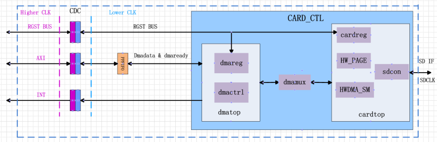
Figure 22-1 CARD Controller Functional Blocks
- dmatop: This block include dmareg and dmactrl modules. It is responsible for control AXI BUS command and data.
- dmareg: This module control dma register read and write operation.
- dmactrl: This module control AXI BUS command and data response.
- cardtop: This block include cardreg, sdcon, HWDMA_SM and HW_PAGE modules.
- cardreg: This module controls pio mode read and write operations.
- sdcon: This module controls device interface protocol.
- HWDMA_SM: This module controls HW DMA mode read and write operations state machine.
- HW_PAGE: This module controls HW DMA mode sector address/page number and block address/page number update in the read/write operations.
22.3 Data Transfer Format
According 1 bit, 4 bit and 8bit mode with trigger in rising edge or both edge, the data transfer have 5 modes. (8 bit mode only be support in EMMC case)
22.3.1 1 bit Bus SDR
1 bit Bus SDR (Single Data Rate): The rising edge sampling can be done by simply using one data signal pin (Data 0). Please refer to figure 22-2.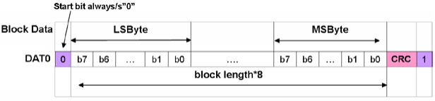
Figure 22-2 1 bit Bus SDR Data Format
22.3.2 4 bit Bus SDR
4 bit Bus SDR: With rising edge sampling, four data signal pins are required (Data 0 ~ Data 3). Please refer to figure 22-3.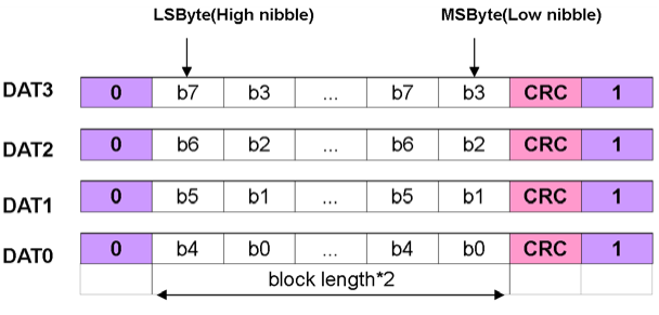
Figure 22-3 4 bit Bus SDR Data Format
22.3.3 8 bit Bus SDR
8 bit Bus SDR: With rising edge sampling, it need to use eight data signal pins (Data 0 ~ Data 7)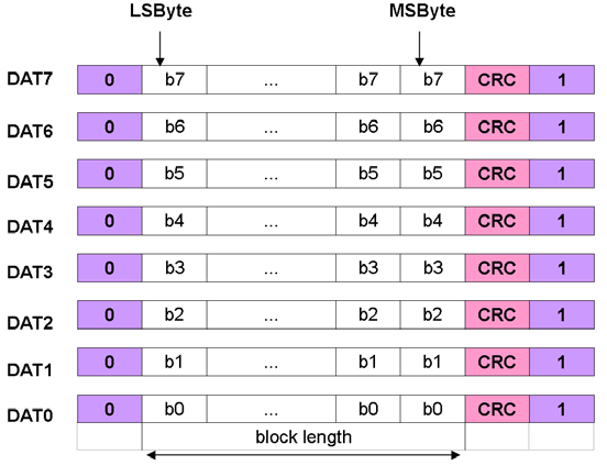
Figure 22-4 8 bit Bus SDR Data Format
22.3.4 4 bit Bus DDR
4 bit Bus DDR (Double Data Rate): Block and CRC are sampled at the rising and falling edges of CLK, while the start and end bits are sampled only at the rising edge. Please refer to figure 22-4.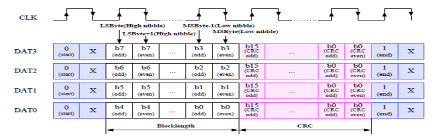
Figure 22-5 4 bit Bus DDR Data Format
22.3.5 8 bit Bus DDR
8 bit Bus DDR (Double Data Rate): Using eight data signal pins (Data 0 ~ Data 7), the data transfer mode is like 4 bit Bus DDR. Please refer to figure 22-5.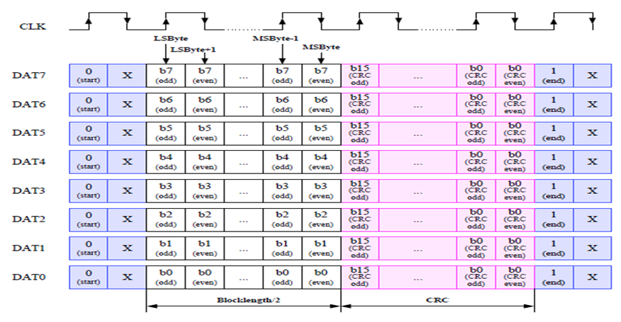
Figure 22-6 8 bit Bus DDR Data Format
22.4 Data Transfer Mode
The EMMC module supports PIO/DMA/HWDMA mode. Please refer to register map chapter for the setting.
The SD/SDIO module only support PIO and DMA mode. Please refer to register map chapter for the setting.
22.5 Function Output Port Setting
When the Group1.1 register bit5 set to "1", the EMMC function port will output to SP7021 pin88~97.
When the Group1.1 register bit6 set to "1", the SDCARD function port will output to SP7021 pin81~86.
The SDIO function port can be output to any pins of GPIO port1~8 by set Group2.11~2.13 registers. (Please refer to chapter5 for detail pinmux setting)
22.6 Baud Rate Generation
The baud rate setting for EMMC/SD/SDIO modules are SDCLK = DPLL_CLK / (sdfqsel + 1).
The sdfqsel value can be set in Group119.4[31:20], Group126.17[11:0] and Group265.17[11:0] for EMMC, SD and SDIO modules.
22.7 Adjust Timing Principle
The basic principle is to offset the latency caused by path delay and device output delay by configuring the three parameters clk_delay, wr_delay, and rd_delay. It should be noted that EMMC/SD/SDIO should distinguish between default speed and high speed during TX operation. When RX is operated, only the SD/SDIO needs to distinguish between default speed and high speed. EMMC does not distinguish between RX and high speed. The adjust timing principle as below description and figure 22-7&8 show the Default speed SDR mode write and read delay timing status.
- SD/SDIO/EMMC default speed
- write operation(The controller is sent with the negative edge SD_CLK, and the device is sampled using the positive edge SD_CLK)
- When path_clk_delay > path_data_delay, path_data_delay+wr_delay=path_clk_delay
- When path_clk_delay < path_data_delay, path_clk_delay+clk_delay=path_data_delay
- read operation(The controller samples with negative edge SD_CLK, and the device sends with positive edge SD_CLK)
- path_clk_delay + Tout_delay + path_data_delay = rd_delay +SD_CLK/2
- write operation(The controller is sent with the negative edge SD_CLK, and the device is sampled using the positive edge SD_CLK)
- SD/SDIO/EMMC high speed
- write operation(The controller is sent with the positive edge SD_CLK, and the device is sampled with the positive edge SD_CLK)
- path_data_delay+wr_delay=path_clk_delay + SD_CLK/2
- read operation(The controller is sampled with positive edge SD_CLK and the device is sent with positive edge SD_CLK)
- path_clk_delay + Tout_delay + path_data_delay = rd_delay
- write operation(The controller is sent with the positive edge SD_CLK, and the device is sampled with the positive edge SD_CLK)
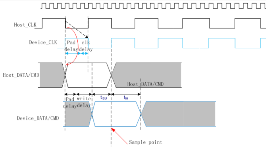
Figure 22-7 Default speed SDR mode write delay timing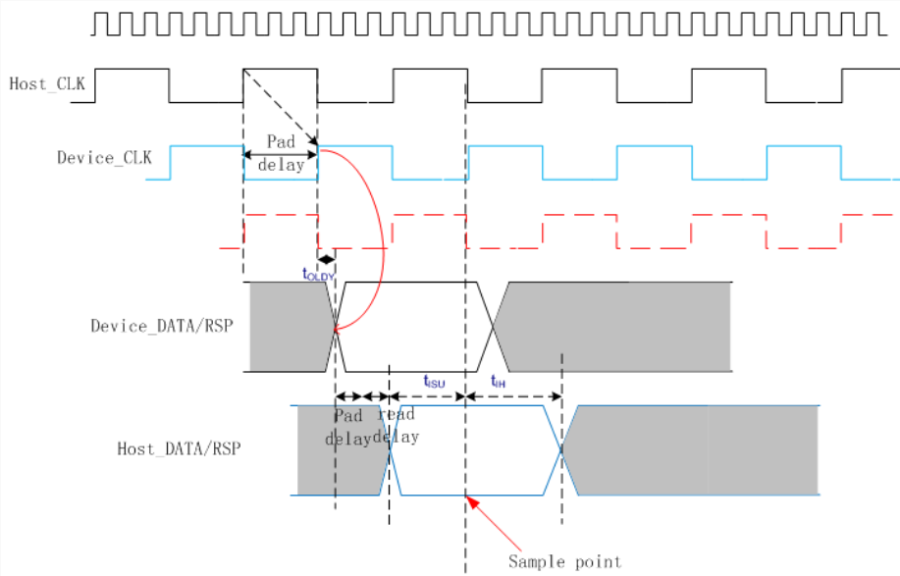
Figure 22-8 Default speed SDR mode read delay timing
Please refer to register map chapter for the clock/write/read delay timing setting.
22.8 CARD_CTL Interrupts
EMMC_CTL support three type interrupts which include pio_int, dma_int and hw_dma _int. SD/SDIO only support two type interrupts which include pio_int and dma_int.
HW DMA can be enable at Group118.4 register bit1. Pio mode and DMA mode can be select at Group119.4 register bit0.
Figure 22-9 shows the EMMC interrupt tree, figure 22-10 shows the SD/SDIO interrupt tree. The interrupt status can be read from registers. Please refer to register map chapter. 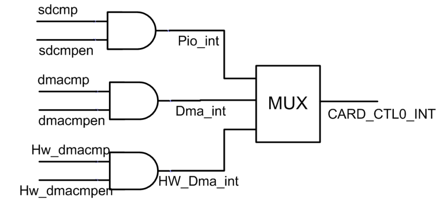
Figure 22-9 EMMC Interrupt Tree
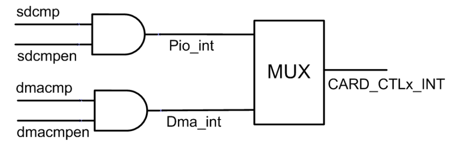
Figure 22-10 SD/SDIO Interrupt Tree
22.9 Register Map
22.9.1 Registers Memory Map
CARD0 Register Memory Map
Memory Map Start Address | Data Width | Group No. | Module |
|---|---|---|---|
| 0x9C003B00 | 32 | 118 | CARD0 |
| 0x9C003B80 | 32 | 119 | CARD0 |
| 0x9C003C00 | 32 | 120 | CARD0 |
CARD1 Register Memory Map
Memory Map Start Address | Data Width | Group No. | Module |
|---|---|---|---|
| 0x9C003E80 | 32 | 125 | CARD1 |
| 0x9C003F00 | 32 | 126 | CARD1 |
| 0x9C003F80 | 32 | 127 | CARD1 |
| 0x9C004000 | 32 | 128 | CARD1 |
| 0x9C004080 | 32 | 129 | CARD1 |
| 0x9C008400 | 32 | 264 | CARD4 |
| 0x9C008480 | 32 | 265 | CARD4 |
| 0x9C008500 | 32 | 266 | CARD4 |
| 0x9C008580 | 32 | 267 | CARD4 |
| 0x9C008600 | 32 | 268 | CARD4 |
CARD1 and CARD4 registers have the same offset in corresponding register group. Only CARD1 registers are described in following register description, for CARD4 please refer to CARD1 description for more detail.
22.9.2 Registers Description
RGST Table Group 118 CARD CTL: HW General Config
118.0 Card Media Type And DMA Source/Destination (card mediatype srcdst)
Address: 0x9C003B0
Reset: 0x0
Field Name | Bit | Access | Description |
Reserved | 31:16 | RO | RESERVED |
Reserved | 15:11 | RO | RESERVED |
dmadst | 10:8 | RW | DMA Destination Selection others: reserved |
Reserved | 7 | RO | RESERVED |
dmasrc | 6:4 | RW | DMA Source Selection others: reserved |
Reserved | 3 | RO | RESERVED |
MediaType | 2:0 | RW | The Storage Media Type Selection others : reserved |
118.1 CPU Page Count (card cpu page cnt)
Address: 0x9C003B04
Reset: 0x0000 0000
Field Name | Bit | Access | Description |
| Reserved | 31:16 | RO | RESERVED |
| CARD CTL PAGE CNT | 15:0 | RO | Page Number that CARD CTL is Reading/Writing Currently |
118.2 Length of SDRAM Sector 0 (sdram sector 0 size)
Address: 0x9C003B08
Reset: 0x0000 FFFF
Field Name | Bit | Access | Description |
| Reserved | 31:16 | RO | RESERVED |
SDRAM SECTOR 0 SIZE | 15:0 | RW | The Length of Sector 0 in SDRAM The actual size equals SDRAM SECTOR 0 SIZE + 1, the unit is page(512 bytes) Note: this sector register can only used in HW DMA mode default is '0xffff' |
118.3 DMA Base Address 32 bits (dma base addr[31:0])
Address: 0x9C003B0C
Reset: 0x0
Field Name | Bit | Access | Description |
DMA BASE ADDR[31:0] | 31:0 | RW | The 32 Bits of DMA Base Address |
118.4 HW DMA Control Signal (HW DMA CTRL)
Address: 0x9C003B10
Reset: 0x0
Field Name | Bit | Access | Description |
| HWSD CMD13 RCA | 31:16 | RW | The Relative Card Address This register is used for the argument of cmd13 when HW DMA EN & HW SD CMD13 EN equals '1' |
| Reserved | 15:14 | RO | RESERVED |
| HW BLOCK NUM | 13:12 | RW | HW DMA Block Number The actual Blcok number is (HW BLOCK NUM+1). |
| dmastart | 11 | WO | HW DMA Start HW DMA EN=1, write 1 to this bit will trigger a hardware speedup multi page DMA data transfer cycle. |
| dmaidle | 10 | RW | DMA Idle 0: Normal state(default) 1: Idle state (reset the DMA operation) |
| HW DMA RST | 9 | WO | HW DMA Rst Write 1 to this field will reset the HW DMA(HW State Ma- chine) function |
| STOP DMA FLAG | 8 | RUW | HW DMA Stop Write 1 to this field will trigger Stop HW DMA function, and this bit will be cleared when sdrst ,HW DMA RST or dmacmpsclr reg |
| Reserved | 7 | RO | RESERVED |
| HW SD CMD13 EN | 6 | RW | Multi Block Transfer CMD13 Enable High active,it is suggested that setting this bit to 1, default is '0', only multi block transfer use |
HW SD DMA TYPE | 5:4 | RW | SD Hardware Type of DMA Mode |
HW SD HCSD EN | 3 | RW | High Capacity Card enable |
Reserved | 2 | RO | RESERVED |
HW DMA EN | 1 | RW | HW DMA Function Enable |
Reserved | 0 | RO | RESERVED |
118.5 Clock Gated Disable (CARD GCLK DISABLE)
Address: 0x9C003B14
Reset: 0x0
Field Name | Bit | Access | Description |
| Reserved | 31:16 | RO | RESERVED |
| Reserved | 15:12 | RO | RESERVED |
| REG CARD REG FREE | 11 | RW | GCLKDIVCARD CARD REG Free run set this bit to 1 will make GCLKDIVCARD CARD REG clock free run,no longer clock gating |
| REG DMA REG FREE | 10 | RW | GCLKDIVCARD DMA REG Free run have the same usage with GCLKDIVCARD CARD REG |
| Reserved | 9 | RO | RESERVED |
| REG SD HWDMA FREE | 8 | RW | GCLKDIVCARD SD HWDMA Free run have the same usage with GCLKDIVCARD CARD REG |
| REG HW DMA FREE | 7 | RW | GCLKDIVCARD HW DMA Free run have the same usage with GCLKDIVCARD CARD REG |
| REG HWDMA PAGE FREE | 6 | RW | GCLKDIVCARD HWDMA PAGE Free run have the same usage with GCLKDIVCARD CARD REG |
| REG DMA CTL FREE | 5 | RW | GCLKDIVCARD DMA CTL Free run have the same usage with GCLKDIVCARD CARD REG |
REG DMA FIFO FREE | 4 | RW | GCLKDIVCARD DMA FIFO Free run |
Reserved | 3 | RO | RESERVED |
Reserved | 2 | RO | RESERVED |
REG SD FREE | 1 | RW | GCLKDIVCARD SD Free run |
REG SD CTL FREE | 0 | RW | GCLKDIVCARD SD CTL Free run |
118.6 Start Address of SDRAM Sector 1 (SDRAM SECTOR 1 ADDR)
Address: 0x9C003B18
Reset: 0x0
Field Name | Bit | Access | Description |
SDRAM SECTOR 1 ADDR | 31:0 | RW | The Start Address of Sector 1 in SDRAM Note: this sector register can only used in HW DMA mode,and when Ring Buffer disable. |
118.7 Length of SDRAM Sector 1 (SDRAM SECTOR 1 SIZE[15:0])
Address: 0x9C003B1C
Reset: 0x0
Field Name | Bit | Access | Description |
| Reserved | 31:16 | RO | RESERVED |
SDRAM SECTOR 1 SIZE | 15:0 | RW | Length of Sector 1 in SDRAM The actual size equals SECTOR 1 SIZE + 1, the unit is page(512 bytes) Note: this sector register can only used in HW DMA mode,and when Ring Buffer disable. |
118.8 Start Address of SDRAM Sector 2 (SDRAM SECTOR 2 ADDR)
Address: 0x9C003B20
Reset: 0x0
Field Name | Bit | Access | Description |
| SDRAM SECTOR 2 ADDR | 31:0 | RW | The Start Address of Sector 2 in SDRAM The usage of this register is same as SDRAM SECTOR 1 ADDR |
118.9 Length of SDRAM Sector 2 (SDRAM SECTOR 2 SIZE[15:0])
Address: 0x9C003B24
Reset: 0x0
Field Name | Bit | Access | Description |
| Reserved | 31:16 | RO | RESERVED |
| SDRAM SECTOR 2 SIZE | 15:0 | RW | Length of Sector 2 in SDRAM The usage of this register is same as SDRAM SECTOR 1 SIZE |
118.10 Start Address of SDRAM Sector 3 (SDRAM SECTOR 3 ADDR)
Address: 0x9C003B28
Reset: 0x0
Field Name | Bit | Access | Description |
| SDRAM SECTOR 3 ADDR | 31:0 | RW | The Start Address of Sector 3 in SDRAM The usage of this register is same as SDRAM SECTOR 1 ADDR |
118.11 Length of SDRAM Sector 3 (SDRAM SECTOR 3 SIZE[15:0])
Address: 0x9C003B2C
Reset: 0x0
Field Name | Bit | Access | Description |
| Reserved | 31:16 | RO | RESERVED |
| SDRAM SECTOR 3 SIZE | 15:0 | RW | Length of Sector 3 in SDRAM The usage of this register is same as SDRAM SECTOR 1 SIZE |
118.12 Start Address of SDRAM Sector 4 (SDRAM SECTOR 4 ADDR)
Address: 0x9C003B30
Reset: 0x0
Field Name | Bit | Access | Description |
| SDRAM SECTOR 4 ADDR | 31:0 | RW | The Start Address of Sector 4 in SDRAM The usage of this register is same as SDRAM SECTOR 1 ADDR |
118.13 Length of SDRAM Sector 4 (SDRAM SECTOR 4 SIZE[15:0])
Address: 0x9C003B34
Reset: 0x0
Field Name | Bit | Access | Description |
| Reserved | 31:16 | RO | RESERVED |
| SDRAM SECTOR 4 SIZE | 15:0 | RW | Length of Sector 4 in SDRAM The usage of this register is same as SDRAM SECTOR 1 SIZE |
118.14 Start Address of SDRAM Sector 5 (SDRAM SECTOR 5 ADDR)
Address: 0x9C003B38
Reset: 0x0
Field Name | Bit | Access | Description |
| SDRAM SECTOR 5 ADDR | 31:0 | RW | The Start Address of Sector 5 in SDRAM The usage of this register is same as SDRAM SECTOR 1 ADDR |
118.15 Length of SDRAM Sector 5 (SDRAM SECTOR 5 SIZE[15:0])
Address: 0x9C003B3C
Reset: 0x0
Field Name | Bit | Access | Description |
| Reserved | 31:16 | RO | RESERVED |
| SDRAM SECTOR 5 SIZE | 15:0 | RW | Length of Sector 5 in SDRAM The usage of this register is same as SDRAM SECTOR 1 SIZE |
118.16 Start Address of SDRAM Sector 6 (SDRAM SECTOR 6 ADDR)
Address: 0x9C003B40
Reset: 0x0
Field Name | Bit | Access | Description |
| SDRAM SECTOR 6 ADDR | 31:0 | RW | The Start Address of Sector 6 in SDRAM The usage of this register is same as SDRAM SECTOR 1 ADDR |
118.17 Length of SDRAM Sector 6 (SDRAM SECTOR 6 SIZE[15:0])
Address: 0x9C003B44
Reset: 0x0
Field Name | Bit | Access | Description |
| Reserved | 31:16 | RO | RESERVED |
| SDRAM SECTOR 6 SIZE | 15:0 | RW | Length of Sector 6 in SDRAM The usage of this register is same as SDRAM SECTOR 1 SIZE |
118.18 Start Address of SDRAM Sector 7 (SDRAM SECTOR 7 ADDR)
Address: 0x9C003B48
Reset: 0x0
Field Name | Bit | Access | Description |
| SDRAM SECTOR 7 ADDR | 31:0 | RW | The Start Address of Sector 7 in SDRAM The usage of this register is same as SDRAM SECTOR 1 ADDR |
118.19 Length of SDRAM Sector 7 (SDRAM SECTOR 7 SIZE[15:0])
Address: 0x9C003B4C
Reset: 0x0
Field Name | Bit | Access | Description |
| Reserved | 31:16 | RO | RESERVED |
| SDRAM SECTOR 7 SIZE | 15:0 | RW | Length of Sector 7 in SDRAM The usage of this register is same as SDRAM SECTOR 1 SIZE |
118.20 SDRAM Sector Counter (sdram sector cnt)
Address: 0x9C003B50
Reset: 0x0
Field Name | Bit | Access | Description |
| HW PAGE CNT | 31:16 | RO | HW DMA Page Count Indicate which page is being read or written, used in HW DMA mode. |
| Reserved | 15:5 | RO | RESERVED |
HW BLOCK CNT | 4:3 | RO | HW DMA Block Counter for wait handshake signal from Flash Memory |
SDRAM SECTOR CNT | 2:0 | RO | SDRAM Sector Count |
118.21 32bits of HW DMA Start Page Address of Block0 (dma hw page addr 0[31:0])
Address: 0x9C003B54
Reset: 0x0
Field Name | Bit | Access | Description |
HW PAGE ADDR 0[31:0] | 31:0 | RW | 32 Bits of Start Page Address of the 1st Block |
118.22 32bits of HW DMA Start Page Address of Block1 (dma hw page addr 1[31:0])
Address: 0x9C003B58
Reset: 0x0
Field Name | Bit | Access | Description |
HW PAGE ADDR 1[31:0] | 31:0 | RW | 32 Bits of Start Page Address of the 2nd Block |
118.23 32bits of HW DMA Start Page Address of Block2 (dma hw page addr 2[31:0])
Address: 0x9C003B5C
Reset: 0x0
Field Name | Bit | Access | Description |
| HW PAGE ADDR 2[31:0] | 31:0 | RW | 32 Bits of Start Page Address of the 3rd Block |
118.24 32bits of HW DMA Start Page Address of Block3 (dma hw page addr 3[31:0])
Address: 0x9C003B60
Reset: 0x0
Field Name | Bit | Access | Description |
| HW PAGE ADDR 3[31:0] | 31:0 | RW | 32 Bits of Start Page Address of the 4th Block |
118.25 HW DMA Page Number of Block0 (dma hw page num0)
Address: 0x9C003B64
Reset: 0x0
Field Name | Bit | Access | Description |
| Reserved | 31:16 | RO | RESERVED |
| HW PAGE NUM0 | 15:0 | RW | Declare how many pages will be read or write start from the start page address of block0 The actual operation page number is (HW PAGE NUM0+1) |
118.26 HW DMA Page Number of Block1 (dma hw page num1)
Address: 0x9C003B68
Reset: 0x0
Field Name | Bit | Access | Description |
| Reserved | 31:16 | RO | RESERVED |
| HW PAGE NUM1 | 15:0 | RW | Declare how many pages will be read or write start from the start page address of block1 The actual page number is (HW PAGE NUM1 +1) |
118.27 HW DMA Page Number of Block2 (dma hw page num2)
Address: 0x9C003B6C
Reset: 0x0
Field Name | Bit | Access | Description |
| Reserved | 31:16 | RO | RESERVED |
| HW PAGE NUM2 | 15:0 | RW | Declare how many pages will be read or write start from the start page address of block2 The actual page number is (HW PAGE NUM2 +1) |
118.28 HW DMA Page Number of Block3 (dma hw page num3)
Address: 0x9C003B70
Reset: 0x0
Field Name | Bit | Access | Description |
| Reserved | 31:16 | RO | RESERVED |
| HW PAGE NUM3 | 15:0 | RW | Declare how many pages will be read or write start from the start page address of block3 The actual page number is (HW PAGE NUM3 +1) |
118.29 32 Bits of HW Wait Number (dma hw wait num[31:0])
Address: 0x9C003B74
Reset: 0xFFFF FFFF
Field Name | Bit | Access | Description |
HW WAIT NUM[31:0] | 31:0 | RW | HW Wait Number 32 Bits 32 bits of wait cycles number in the hardware speedup DMA(HW DMA mode). |
118.30 HW Delay Number (dma hw delay num)
Address: 0x9C003B78
Reset: 0x0000 003F
Field Name | Bit | Access | Description |
| Reserved | 31:16 | RO | RESERVED |
| HW DELAY NUM | 15:0 | RW | HW Delay Number Delay cycles number in the hardware speedup DMA(HWDMA mode). |
118.31 Debug signals for dma mode (Reserved)
Address: 0x9C003B7C
Reset: 0x0
Field Name | Bit | Access | Description |
| Reserved | 31:25 | RO | RESERVED |
| Reserved | 24:22 | RO | RESERVED |
| Reserved | 21:11 | RO | RESERVED |
| Reserved | 10:0 | RO | RESERVED |
RGST Table Group 119 CARD CTL: SD controller
119.0 EMMC Boot Operation Control (boot ctrl)
Address: 0x9C003B80
Reset: 0x0
Field Name | Bit | Access | Description |
Reserved | 31:8 | RO | RESERVED |
bootack | 7:5 | RO | Boot Ack Value |
boot mode | 4 | RUW | EMMC Have Boot Operation |
fast boot | 3 | RW | Use Fast Boot Start Boot Operation |
boot data tmr | 2 | RW | Boot Data Timeout For 1s |
boot ack tmr | 1 | RW | Boot Ack Timeout For 50ms |
boot ack en | 0 | RW | Boot Ack In Boot Mode |
119.1 SD Voltage Register (sd vol ctrl)
Address: 0x9C003B84
Reset: 0x0000 0003
Field Name | Bit | Access | Description |
| Reserved | 31:6 | RO | RESERVED |
vol result | 5:4 | RO | HW Switch Voltage Sequence Result |
hw set vol | 3 | RW | HW set Voltage to 1.8v |
sw set vol | 2 | RW | Software set Voltage to 1.8v |
vol tmr | 1:0 | RW | Timeout for 1ms(hw set vol) |
119.2 SD INT Control (sd int)
Address: 0x9C003B88
Reset: 0x0
Field Name | Bit | Access | Description |
| Reserved | 31:12 | RO | RESERVED |
| hw dma cmp clr | 11 | WU | Write 1 to this bit clear HW DMA interrupt flag |
| HW DMA CMP | 10 | RO | HW DAM Complete interrupt flag |
| hw dma cmp en | 9 | RW | HW DMA Data Transfer Complete Interrupt Enable 0: Disable the HW DMA data transfer complete interrupt(default) |
| DETECT INT CLR | 8 | WU | Clear card detect interrupt |
DETECT INT | 7 | RO | Card plug-in or pull-out interrupt |
DETECT INT EN | 6 | RW | Card plug-in or pull-out interrupt enable |
sdio int clr | 5 | WU | Clear SDIO interrupt register in SDIO host |
sdio int | 4 | RO | SDIO interrupt from SDIO card |
sdio int en | 3 | RW | Enable SDIO Interrupt |
sd cmp clr | 2 | WO | Clear SD cmp Interrupt |
sd cmp | 1 | RO | SD Operation Complete Interrupt |
sdcmpen | 0 | RW | Enable SD Interrupt |
119.3 SD Page number for this transfer (sd page num)
Address: 0x9C003B8C
Reset: 0x0
Field Name | Bit | Access | Description |
| Reserved | 31:16 | RO | RESERVED |
| sd page num | 15:0 | RUW | The total Tx/Rx page number in the cmd(only for normal DMA and PIO mode). When config, it indicate how many pages will be read or write. The actual operation page number is ( PAGE NUM+ 1 ) When read, it indicate which page is being read or written, from page*(PAGE NUM) to page*0 default is '0' |
119.4 SD Controller transaction mode select (sd config0)
Address: 0x9C003B90
Reset: 0x0030 30C0
Field Name | Bit | Access | Description |
| sdfqsel | 31:20 | RW | SD Controller Clock Frequency division selection SDCLK = DPLL CLK/(sdfqsel + 1) 0x0 : not support 0x1 : 2-div 0x2 : 3-div 0x3 : 4-div(default) others : reserved |
| selci | 19 | RW | SDCLK Selection default is '0' |
| mmc8 en | 18 | RW | MMC 8Bit Mode Enable, only for MMC card with 8bit bus 0x0: Data bus width controled by bit 10 of this register; when mmc8 en disable, the controller can only select 1bit bus or 4bit bus width(default) 0x1: 8bit data bus; when mmc8 en enable, the bit10 of this register will be ignored |
| detect tmr | 17:16 | RW | Card Detect timmer for 1s 0x0: 18'h61a8 (25000*(1/25Mhz) = 1ms)(default) 0x1: 18'hc350 (50000*(1/50Mhz) = 1ms) 0x2: 18'h186a0(100000*(1/100Mhz) = 1ms) 0x3: 18'h320c8(205000*(1/202Mhz) = 1ms) This should be set before operation for detect card plug-in or pull-out |
sdrsptype | 15 | RW | SD Controller Response Type |
rx4 en | 14 | RW | PIO Mode Rx Buffer 4Byte Enable |
sdcrctmren | 13 | RW | SD Controller CRC Timer Enable |
sdrsptmren | 12 | RW | SD Controller Response Timer Enable |
sddatawd | 11 | RW | SD Controller Data Bus Width |
sdmmcmode | 10 | RW | Card Mode1 |
sdiomode | 9 | RW | Card Mode2 |
sdrspchk en | 8 | RW | HW check Response CRC7 |
sdcmddummy | 7 | RW | Auto Tx Dummy after Cmd |
sdautorsp | 6 | RW | Auto Response after Cmd |
sd trans mode | 5:4 | RW | Transaction Mode Select |
ddr rx first hcyc | 3 | RW | DDR Mode RX First Byte Data Remain Half Cycle |
sd len mode | 2 | RW | SD Length is Specified |
sdddrmode | 1 | RW | SD DDR Mode Enable |
sdpiomode | 0 | RW | SD PIO Mode Enable |
119.5 SDIO Controller Reset (sdio ctrl)
Address: 0x9C003B94
Reset: 0x0
Field Name | Bit | Access | Description |
| Reserved | 31:7 | RO | RESERVED |
INT MULTI TRIG | 6 | RW | SDIO Interrupt Trigger Multiple time 0:When SDIO device send interrupt to controller,every interrupt only send one time(default) |
SUS DATA FLAG | 5 | WO | Write 1 to Suspend SD state machine |
CON REQ | 4 | WO | write 1 to trigger SD state machine continue, and SDIO |
SUS REQ | 3 | WO | write 1 to trigger SD state machine end |
RESU | 2 | WO | write 1 to trigger SD state machine to restore and also resume SDIO interrupt period generation rightly |
S4MI | 1 | RW | trigger interrupt period generation between 4-bit read blocks |
RWC | 0 | RW | Read Wait Control signal |
119.6 SD Controller Reset (sd rst)
Address: 0x9C003B98
Reset: 0x0
Field Name | Bit | Access | Description |
Reserved | 31:3 | RO | RESERVED |
sdiorst | 2 | WO | SDIO Controller Interrupt Register Reset |
sdcrcrst | 1 | WO | SD Controller CRC Reset |
sdrst | 0 | WO | SD Controller Software Reset |
119.7 SD Controller Control Signal (sd ctrl)
Address: 0x9C003B9C
Reset: 0x0
Field Name | Bit | Access | Description |
| Reserved | 31:4 | RO | RESERVED |
| emmcctrl | 3 | WO | Start Boot Operation Trigger Signal Writting 1 to this bit will generate trigger signal for start boot operation (emmc use only) |
| sdioctrl | 2 | WO | Dummy clock Trigger Signal Writting 1 to this bit will generate trigger signal for trans- mitting dummy clock in IDLE state (sdio use only) |
| sdctrl[1] | 1 | WO | Dummy clock Trigger Signal Writting 1 to this bit will generate trigger signal for trans- mitting dummy clock The dummy cycle number config in sd tx dummy num register |
| sdctrl[0] | 0 | WO | New Command Trigger Signal Writting 1 to this bit will generate trigger signal for starting transaction |
119.8 SD Controller Status (Sd Status)
Address: 0x9C003BA0
Reset: 0x0000 c035
Field Name | Bit | Access | Description |
| Reserved | 31:19 | RO | RESERVED |
| sdstatus | 18:0 | RO | SD Controller Status bit0 : Dummy ready bit1 : Response buffer full, high active bit2 : Transmitted data buffer empty, high active bit3 : Receive data buffer full, high active bit4 : Status of pin cmd bit5 : Status of pin SD data0 bit6 : Timeout flag of waiting response, high active bit7 : Timeout flag of waiting card's CRC check result, high active bit8 : Wait STB(start bit) timeout, when read data from card bit9 : Rsp crc7 error bit10: CRC Token Check error bit11: Rdata CRC16 error(all CRC16) bit12: Suspend state ready bit13: Busy cycle bit14: Status of pin SD data1 bit15: Status of SD SENSE bit16: Timeout flag of waiting boot ack, high active bit17: Timeout flag of waiting boot data, high active bit18: EMMC boot ack error, high active |
119.9 SD Controller State Machine (Sd State)
Address: 0x9C003BA4
Reset: 0x0000 4000
Field Name | Bit | Access | Description |
| Reserved | 31:15 | RO | RESERVED |
| sdstate new | 14:8 | RO | New SD state machine of SD Controller bit14 : 0: Transaction have no finish or idle 1: Transaction finish or idle(default) bit13 : 0: Transaction have no error or timeout(default) 1: Transaction error or timeout bit12:8 : represent the state machine other states,don't care |
| Reserved | 7 | RO | RESERVED |
| sdcrdcrc | 6:4 | RO | The CRC Token Check Result 0x0 : reserved(default) 0x2 : CRC check correct 0x5 : CRC check incorrect others: reserved |
| Reserved | 3 | RO | RESERVED |
| sdstate | 2:0 | RO | State Machine of SD Controller 0x0 : Idle(default) 0x1 : Transmit Dummy Clock 0x2 : Transmit SD Command 0x3 : Receiveing SD Response 0x4 : Transmitting Data 0x5 : Receiving CRC Token 0x6 : Receiving Data 0x7 : reserved |
119.10 Hardware SD State Machine (sd hw state)
Address: 0x9C003BA8
Reset: 0x0
Field Name | Bit | Access | Description |
| Reserved | 31:10 | RO | RESERVED |
| HWSD SM | 9:0 | RO | The Hardware SD State bit6: SD HW DMA Error bit7: SD HW DMA Done Note: when this register equals '0', it means sd controller in idle state. |
119.11 SD Controller Data Length (sd blocksize)
Address: 0x9C003BAC
Reset: 0x0000 01FF
Field Name | Bit | Access | Description |
| Reserved | 31:11 | RO | RESERVED |
| sd data len | 10:0 | RW | Data Length of One Block The actual length equals (sddatalen + 1) 0x0 : 1 byte 0x1 : 2 byte ... 0x1ff : 512 byte(default) ... 0x7ff : 2048 byte |
119.12 SD Controller config (sd config1)
Address: 0x9C003BB0
Reset: 0x5FF0 4007
Field Name | Bit | Access | Description |
sd high speed en | 31 | RW | SD Controller High Speed Mode Enable Include HS, SDR mode with UHS-I, HS200. High active. default is '0' Note: this bit will change the send/sample edge of sdclk. If enable, the controller send cmd/data at rising edge of sdclk, and sample rsp/data at rising edge of sdclk; If disable, the controller send cmd/data at falling edge of sdclk, and sample rsp/data at falling edge of sdclk for SD/SDIO If enable, the 'delay sel' will delay 0∼7*DPLL start from 0∼7*DPLL start from falling edge of sdclk for SD/SDIO |
sdrsptmr | 30:2 | 0 RW | Response Timer It used to calculate the timeout, unit is 1*sdclk default is '0x5ff' |
sdcrctmr | 19:9 | RW | CRC Timer |
TX DUMMY NUM | 8:0 | RW | Dummy Cycle Number |
119.13 SD Controller timing config (sd timing config0)
Address: 0x9C003BB4
Reset: 0x0
Field Name | Bit | Access | Description |
| Reserved | 31:11 | RO | RESERVED |
| sd rd dly sel | 10:8 | RW | Selection Signal of SD Read Delay Delay the time that SD controller sample rsp and data from sd interface, the unit is 1*DPLL 0x0: no delay(default) 0x1: delay 1*DPLL clock 0x2: delay 2*DPLL clock 0x3: delay 3*DPLL clock 0x4: delay 4*DPLL clock 0x5: delay 5*DPLL clock 0x6: delay 6*DPLL clock 0x7: delay 7*DPLL clock |
| Reserved | 7 | RO | RESERVED |
| sd wr dly sel | 6:4 | RW | Selecting Signal of SD Write Delay Delay SD tx cmd/data to card, the unit is 1*DPLL 0x0: no delay(default) 0x1: delay 1*DPLL clock 0x2: delay 2*DPLL clock 0x3: delay 3*DPLL clock 0x4: delay 4*DPLL clock 0x5: delay 5*DPLL clock 0x6: delay 6*DPLL clock 0x7: delay 7*DPLL clock |
| Reserved | 3 | RO | RESERVED |
| sd clk dly sel | 2:0 | RW | Selecting Signal of SD Clock Delay Delay SD clock to card, the unit is 1*DPLL 0x0: no delay(default) 0x1: delay 1*DPLL clock 0x2: delay 2*DPLL clock 0x3: delay 3*DPLL clock 0x4: delay 4*DPLL clock 0x5: delay 5*DPLL clock 0x6: delay 6*DPLL clock 0x7: delay 7*DPLL clock |
119.14 SD Rx Data Timer (sd rx data tmr)
Address: 0x9C003BB8
Reset: 0x0131 2D00
Field Name | Bit | Access | Description |
| Reserved | 31:29 | RO | RESERVED |
| sd rx dat tmr | 28:0 | RW | max timer value selection default value 29'h01321d00 |
119.15 SD PIO Mode TX Data (sd piodatatx)
Address: 0x9C003BBC
Reset: 0x0000 FFFF
Field Name | Bit | Access | Description |
| sd pio data tx | 31:0 | RW | Buffer for Transmitting Data only used in PIO mode, little endian |
119.16 SD PIO Mode RX Data (sd piodatarx)
Address: 0x9C003BC0
Reset: 0x0
Field Name | Bit | Access | Description |
| sd pio data Rx | 31:0 | RO | Buffer for Receiving Data only used in PIO mode When rx4 en enable, read 4Bytes rxdata from sdpiodataRx[31:0], little endian When rx4 en disable, read 2Bytes rxdata from sdpiodataRx[15:0], sdpiodataRx[31:16] are reserved, little endian |
119.17 SD Command Buffer0∼3 (sd cmdbuf[0-3])
Address: 0x9C003BC4
Reset: 0xFFFF FFFF
Field Name | Bit | Access | Description |
| sdcmdbuf[0] | 31:24 | RW | Buffer for Store the 1st Byte of Command Indicate Command[47:40] bits |
| sdcmdbuf[1] | 23:16 | RW | Buffer for Store the 2st Byte of Command Indicate Command[39:32] bits |
| sdcmdbuf[2] | 15:8 | RW | Buffer for Store the 3st Byte of Command Indicate Command[31:24] bits |
| sdcmdbuf[3] | 7:0 | RW | Buffer for Store the 4st Byte of Command Indicate Command[23:16] bits |
119.18 SD Command Buffer4 (sd cmdbuf[4])
Address: 0x9C003BC8
Reset: 0x0000 00FF
Field Name | Bit | Access | Description |
Reserved | 31:8 | RO | |
sdcmdbuf[4] | 7:0 | RW | Buffer for Store the 5nd Byte of Command |
119.19 SD Response Buffer0∼3 (sd rspbuf[0-3])
Address: 0x9C003BCC
Reset: 0x0
Field Name | Bit | Access | Description |
| sdrespbuf0 | 31:24 | RO | Buffer for Store the 1st/7st/13st Byte of Response |
| sdrespbuf1 | 23:16 | RO | Buffer for Store the 2st/8st/14st Byte of Response |
| sdrespbuf2 | 15:8 | RO | Buffer for Store the 3st/9st/15st Byte of Response |
| sdrespbuf3 | 7:0 | RO | Buffer for Store the 4st/10st/16st Byte of Response |
119.20 SD Response Buffer4∼5 (sd rspbuf[4-5])
Address: 0x9C003BD0
Reset:
Field Name | Bit | Access | Description |
Reserved | 31:16 | RO | |
| sdrespbuf4 | 15:8 | RO | Buffer for Store the 5st/11st/17st Byte of Response |
sdrespbuf5 | 7:0 | RO | Buffer for Store the 6st/12st Byte of Response |
119.21 (Reserved)
Address: 0x9C003BD4
Reset: 0x0
Field Name | Bit | Access | Description |
Reserved | 31:0 | RO |
119.22 (Reserved)
Address:0x9C003BD8
Reset:
Field Name | Bit | Access | Description |
Reserved | 31:0 | RO |
119.23 (Reserved)
Address: 0x9C003BDC
Reset:
Field Name | Bit | Access | Description |
Reserved | 31:0 | RO |
119.24 (Reserved)
Address: 0x9C003BE0
Reset:
Field Name | Bit | Access | Description |
Reserved | 31:0 | RO |
119.25 (Reserved)
Address: 0x9C003BE4
Reset:
Field Name | Bit | Access | Description |
Reserved | 31:0 | RO |
119.26 (Reserved)
Address: 0x9C003BE8
Reset:
Field Name | Bit | Access | Description |
Reserved | 31:0 | RO |
119.27 (Reserved)
Address: 0x9C003BEC
Reset:
Field Name | Bit | Access | Description |
Reserved | 31:0 | RO |
119.28 (Reserved)
Address: 0x9C003BF0
Reset:
Field Name | Bit | Access | Description |
Reserved | 31:0 | RO |
119.29 (Reserved)
Address: 0x9C003BF4
Reset:
Field Name | Bit | Access | Description |
Reserved | 31:0 | RO |
119.30 (Reserved)
Address: 0x9C003BF8
Reset:
Field Name | Bit | Access | Description |
Reserved | 31:0 | RO |
119.31 (Reserved)
Address: 0x9C003BFC
Reset:
Field Name | Bit | Access | Description |
Reserved | 31:0 | RO |
RGST Table Group 120 CARD CTL: MS controller
120.0 MS Controller Write Data Buffer0 (ms wd data[0])
Address: 0x9C003C00
Reset: 0x0
Field Name | Bit | Access | Description |
Reserved | 31:8 | RO | |
msdata0 | 7:0 | RW | MS Controller Register of Write Data0 |
120.1 MS Controller Write Data Buffer1 (ms wd data[1])
Address: 0x9C003C04
Reset: 0x0
Field Name | Bit | Access | Description |
Reserved | 31:8 | RO | |
msdata1 | 7:0 | RW | MS Controller Register of Write Data1 |
120.2 MS Controller Write Data Buffer2 (ms wd data[2])
Address: 0x9C003C08
Reset: 0x0
Field Name | Bit | Access | Description |
Reserved | 31:8 | RO | |
msdata2 | 7:0 | RW | MS Controller Register of Write Data2 |
120.3 MS Controller Write Data Buffer3 (ms wd data[3])
Address: 0x9C003C0C
Reset: 0x0
Field Name | Bit | Access | Description |
Reserved | 31:8 | RO | |
msdata3 | 7:0 | RW | MS Controller Register of Write Data3 |
120.4 MS Controller Write Data Buffer4 (ms wd data[4])
Address: 0x9C003C10
Reset: 0x0
Field Name | Bit | Access | Description |
Reserved | 31:8 | RO | |
msdata4 | 7:0 | RW | MS Controller Register of Write Data4 |
120.5 MS Controller Write Data Buffer5 (ms wd data[5])
Address: 0x9C003C14
Reset: 0x0
Field Name | Bit | Access | Description |
Reserved | 31:8 | RO | |
msdata5 | 7:0 | RW | MS Controller Register of Write Data5 |
120.6 MS Controller Write Data Buffer6 (ms wd data[6])
Address: 0x9C003C18
Reset: 0x0
Field Name | Bit | Access | Description |
Reserved | 31:8 | RO | |
msdata6 | 7:0 | RW | MS Controller Register of Write Data6 |
120.7 MS Controller Write Data Buffer7 (ms wd data[7])
Address: 0x9C003C1C
Reset: 0x0
Field Name | Bit | Access | Description |
Reserved | 31:8 | RO | |
msdata7 | 7:0 | RW | MS Controller Register of Write Data7 |
120.8 MS Controller Write Data Buffer8 (ms wd data[8])
Address: 0x9C003C20
Reset: 0x0
Field Name | Bit | Access | Description |
Reserved | 31:8 | RO | |
msdata8 | 7:0 | RW | MS Controller Register of Write Data8 |
120.9 MS Controller Write Data Buffer9 (ms wd data[9])
Address: 0x9C003C24
Reset: 0x0
Field Name | Bit | Access | Description |
| Reserved | 31:8 | RO | |
| msdata9 | 7:0 | RW | MS Controller Register of Write Data9 Only used to write registers of ms card |
120.10 MS Controller Write Data Buffer10 (ms wd data[10])
Address: 0x9C003C28
Reset: 0x0
Field Name | Bit | Access | Description |
Reserved | 31:8 | RO | |
msdata10 | 7:0 | RW | MS Controller Register of Write Data10 |
120.11 MS Controller Write Data Buffer11 (ms wd data[11])
Address: 0x9C003C2C
Reset: 0x0
Field Name | Bit | Access | Description |
Reserved | 31:8 | RO | |
msdata11 | 7:0 | RW | MS Controller Register of Write Data11 |
120.12 MS Controller Write Data Buffer12 (ms wd data[12])
Address: 0x9C003C30
Reset: 0x0
Field Name | Bit | Access | Description |
Reserved | 31:8 | RO | |
msdata12 | 7:0 | RW | MS Controller Register of Write Data12 |
120.13 MS Controller Write Data Buffer13 (ms wd data[13])
Address: 0x9C003C34
Reset: 0x0
Field Name | Bit | Access | Description |
Reserved | 31:8 | RO | |
msdata13 | 7:0 | RW | MS Controller Register of Write Data13 |
120.14 MS Controller Write Data Buffer14 (ms wd data[14])
Address: 0x9C003C38
Reset: 0x0
Field Name | Bit | Access | Description |
Reserved | 31:8 | RO | |
msdata14 | 7:0 | RW | MS Controller Register of Write Data14 |
120.15 MS Controller Write Data Buffer15 (ms wd data[15])
Address: 0x9C003C3C
Reset: 0x0
Field Name | Bit | Access | Description |
Reserved | 31:8 | RO | |
msdata15 | 7:0 | RW | MS Controller Register of Write Data15 |
120.16 MS Operation Mode and Reset Signal (ms piodmarst)
Address: 0x9C003C40
Reset: 0x0
Field Name | Bit | Access | Description |
Reserved | 31:7 | RO | |
msclrerr | 6 | WO | Clear Signal of Mserror |
mscrcrst | 5 | WO | CRC Buffer Reset |
msreset | 4 | WO | Software Reset |
Reserved | 3:2 | RO | |
HW BLOCK MODE EN | 1 | RW | HW Blcok Level DAM Enable |
mspiomode | 0 | RW | CPU Operation Mode |
120.17 MS TPC Code And Data Size (ms cmd)
Address: 0x9C003C44
Reset: 0x0
Field Name | Bit | Access | Description |
| Reserved | 31:8 | RO | |
| datasize | 7:4 | RW | Data Phase Byte Count The value will be added by 1. Only valid when Read/Write Reg, default is '0' |
| mscommand | 3:0 | RW | Memory Stick Controller TPC Command Register The commands in bracket are only used in MS-Pro,others are used in MS/MS-Pro. 0x2 : READ LONG DATA (READ LONG DATA) 0x3 : Forbidden (READ SHORT DATA) 0x4 : READ REG 0x7 : GET INT 0x8 : SET R/W ADDRS 0x9 : Forbidden (EX SET CMD) 0xb : WRITE REG 0xc : Forbidden (WRITE SHORT DATA) 0xd : WRITE PAGE DATA (WRITE LONG DATA) 0xe : SET CMD others: reserved |
120.18 Reserved (reserved)
Address: 0x9C003C48
Reset: 0x0
Field Name | Bit | Access | Description |
Reserved | 31:0 | RO |
120.19 Hardware MS State (ms hw state)
Address: 0x9C003C4C
Reset: 0x0
Field Name | Bit | Access | Description |
| Reserved | 31:10 | RO | |
| HWMS SM | 9:0 | RO | Hardware MS State bit6 : Hardware MS DMA Error bit7 : Hardware MS DMA Done bit9 : '1' means Hardware DMA is MS write; '0' means Hardware DMA is MS read |
120.20 MS Clock Frequency Configure (ms modespeed)
Address: 0x9C003C50
Reset: 0x0000 00FF
Field Name | Bit | Access | Description |
| Reserved | 31:15 | RO | |
| ms wdat dly sel | 14:12 | RW | Delay Number of MS DATA and MS BS when Write Data to Flash Delay MS tx cmd/data to card, the unit is 1*DPLL 0x0 : no delay(default) 0x1 : delay 1*DPLL clock 0x2 : delay 2*DPLL clock 0x3 : delay 3*DPLL clock 0x4 : delay 4*DPLL clock 0x5 : delay 5*DPLL clock 0x6 : delay 6*DPLL clock 0x7 : delay 7*DPLL clock |
| MS RDY CHK3 EN | 11 | RW | Enable signal for Checking Ready Signal 3 times High active 0 : Check ready signal for 2 times(default) 1 : Check ready signal for 3 times |
| MSType | 10 | RW | Type of MS Card 0 : MS type(default) 1 : MS-Pro type |
| msspeed[8] | 9 | RW | bit8 of msspeed[8:0] default is '0' |
| msdatwd | 8 | RW | MS Interface Mode Selection 0 : Serial mode(default) 1 : 4-bit parallel mode |
| msspeed[7:0] | 7:0 | RW | Clock Frequency of Memory Stick Interface MSCLK = DPLL CLK/(msspeed + 1) 0x0 : not support 0x1 : div-2 0x2 : div-3 .... 0xff: div-256(default) |
120.21 MS Busy Rdy Timer (ms timout)
Address: 0x9C003C54
Reset: 0x0000 001F
Field Name | Bit | Access | Description |
| Reserved | 31:14 | RO | |
| ms rdat dly sel | 13:11 | RW | Delay Number for Read Data Delay the time that MS controller sample rsp and data from MS interface, the unit is 1*DPLL 0x0 : no delay(default) 0x1 : delay 1*DPLL clock 0x2 : delay 2*DPLL clock 0x3 : delay 3*DPLL clock 0x4 : delay 4*DPLL clock 0x5 : delay 5*DPLL clock 0x6 : delay 6*DPLL clock 0x7 : delay 7*DPLL clock |
| ms clk dly sel | 10:8 | RW | Delay Number MS CLK Delay MS clock to card, the unit is 1*DPLL 0x0 : no delay(default) 0x1 : delay 1*DPLL clock 0x2 : delay 2*DPLL clock 0x3 : delay 3*DPLL clock 0x4 : delay 4*DPLL clock 0x5 : delay 5*DPLL clock 0x6 : delay 6*DPLL clock 0x7 : delay 7*DPLL clock |
| Reserved | 7:5 | RO | |
| ms busy rdy timer | 4:0 | RW | The Number of Memory Ticks for Timeout in handshake state default is '0x1f' |
120.22 MS Controller State Machine (Ms State)
Address: 0x9C003C58
Reset: 0x0000 0001
Field Name | Bit | Access | Description |
| Reserved | 31:10 | RO | |
| msstate[9:0] | 9:0 | RO | MS Controller State Machine 0x1 : MSIDLE(default) 0x2 : MSCMD 0x4 : MSWDATA 0x8 : MSWCRC 0x10 : MSRDATA 0x20 : MSRCRC 0x40 : MSBUSY 0x80 : MSREADY 0x100 : MSRCRC POST 0x200 : MS RDY ERR Others : reserved |
120.23 Debug information of MS Controller (Ms Status)
Address: 0x9C003C5C
Reset: 0x0
Field Name | Bit | Access | Description |
Reserved | 31:8 | RO | |
ms data in | 7:4 | RO | Memory Stick Input |
Reserved | 3 | RO | |
msbs | 2 | RU | Memory Stick Controller State Machine |
mserror | 1 | RO | MS Busy Rdy Timeout |
Reserved | 0 | RO |
120.24 Read Data Buffer0 (ms rddata[0])
Address: 0x9C003C60
Reset: 0x0
Field Name | Bit | Access | Description |
| Reserved | 31:8 | RO | |
| rddata | 7:0 | RO | Data0 Read from Card In PIO mode,data and registers of card are in this register the high byte data receive from card registers |
120.25 Read data Buffer1 (ms rddata[1])
Address: 0x9C003C64
Reset: 0x0
Field Name | Bit | Access | Description |
Reserved | 31:8 | RO | |
rddata1 | 7:0 | RO | Data1 read from Card |
120.26 Read Data Buffer2 (ms rddata[2])
Address: 0x9C003C68
Reset: 0x0
Field Name | Bit | Access | Description |
Reserved | 31:8 | RO | |
rddata2 | 7:0 | RO | Data2 Read from Card |
120.27 Read data Buffer3 (ms rddata[3])
Address: 0x9C003C6C
Reset: 0x0
Field Name | Bit | Access | Description |
| Reserved | 31:8 | RO | |
| rddata3 | 7:0 | RO | Data3 Read from Card only used to receive registers of ms card |
120.28 Low Byte of MS Data CRC16 (ms crcbuf[7:0])
Address: 0x9C003C70
Reset:0x0
Field Name | Bit | Access | Description |
| Reserved | 31:16 | RO | |
| mscrc16buf[15:0] | 15:0 | RO | MS Controller CRC Result 16 bits of CRC result |
120.29 High Byte of MS Data CRC16 (ms crcbuf[15:8])
Address: 0x9C003C74
Reset: 0x0
Field Name | Bit | Access | Description |
Reserved | 31:8 | RO | |
mscrc16buf[15:8] | 7:0 | RO | MS Controller CRC Result |
120.30 MS CRC Check Result and Busy Rdy TimeOut (ms crcerror)
Address: 0x9C003C78
Reset: 0x0000 0002
Field Name | Bit | Access | Description |
| Reserved | 31:2 | RO | |
| mscrc16cor | 1 | RO | MS Controller CRC Correct Status 0 : CRC error 1 : CRC correct(default) |
| mserror | 0 | RO | MS error Timeout Occurs when Wait for Ready Signal of Card |
120.31 MS Controller PIO Ready (ms piordy)
Address: 0x9C003C7C
Reset: 0x0
Field Name | Bit | Access | Description |
| Reserved | 31:1 | RO | |
| mspiordy | 0 | RO | PIO Ready Signal for Write/Read High active. When read packet, it shows data is received. When write packet, it shows data is sent out,the next data can be written. |
RGST Table Group 125 CARD CTL: General Config
125.0 Card Media Type (card mediatype)
Address: 0x9C003E80
Reset: 0x0
Field Name | Bit | Access | Description |
| Reserved | 31:16 | RO | |
| Reserved | 15:3 | RO | |
| MediaType | 2:0 | RW | The Storage Media Selection 0x0 : None, low power mode(default) 0x6 : SD memory card 0x7 : Memory Stick others : reserved Note: if operate with SD/MMC/SDIO card, please se- lect '0x6' to enable sd function; if operate with MS/MSPro card, please select '0x7' to enable ms function |
125.1 Reserved (reserved)
Address: 0x9C003E84
Reset: 0x0
Field Name | Bit | Access | Description |
Reserved | 31:0 | RO |
125.2 CPU Page Count (card cpu page cnt)
Address: 0x9C003E88
Reset: 0x0000 FFFF
Field Name | Bit | Access | Description |
| Reserved | 31:16 | RO | |
| CPU PAGE CNT | 15:0 | RW | Page Number that Software is Reading/Writing Currently If SDRAM write to Card, it shows that software is carrying the page data in CPU PAGE CNT to SDRAM. If SDRAM read from Card, it show that software is carrying the page data in CPU PAGE CNT from SDRAM. Note: this register can only used in HW DMA mode, and ring buffer enable. default is '0xffff' |
125.3 CARD CTL Page Count (card ctl page cnt)
Address: 0x9C003E8C
Reset: 0x0
Field Name | Bit | Access | Description |
| Reserved | 31:16 | RO | |
CARD CTL PAGE CNT | 15:0 | RO | Page Number that CARD CTL is Reading/Writing Currently If SDRAM write to Card, it shows that CARD CTL is carrying the page data in CARD CTL PAGE CNT to SDRAM. If SDRAM read from Card, it show that CARD CTL is carrying the page data in CARD CTL PAGE CNT from SDRAM Note: this register can only used in HW DMA mode |
125.4 Length of SDRAM Sector 0 (sdram sector 0 size)
Address: 0x9C003E90
Reset: 0x0000 FFFF
Field NameBitAccessDescription
Reserved31:16RO
Field Name | Bit | Access | Description |
| Reserved | 31:16 | RO | |
SDRAM SECTOR 0 SIZE | 15:0 | RW | The Length of Sector 0 in SDRAM The actual size equals SDRAM SECTOR 0 SIZE + 1, the unit is page(512 bytes) Note: this sector register can only used in HW DMA mode default is '0xffff' |
125.5 Ring Buffer On (RING BUFFER ON)
Address: 0x9C003E94
Reset: 0x0
Field Name | Bit | Access | Description |
| Reserved | 31:16 | RO | |
| Reserved | 15:1 | RO | |
| RING BUFFER ON | 0 | RW | Ring buffer enable 0 : Ring buffer is disable(default). 1 : Ring buffer is enable. Note:HW DMA use only, if ring buffer enable, only the sector 0 in SDRAM will be used. |
125.6 Clock Gated Disable (CARD GCLK DISABLE)
Address: 0x9C003E98
Reset: 0x0
Field Name | Bit | Access | Description |
| Reserved | 31:16 | RO | |
| Reserved | 15:12 | RO | |
| REG CARD REG FREE | 11 | RW | GCLKDIVCARD CARD REG Free run set this bit to 1 will make GCLKDIVCARD CARD REG clock free run,no longer clock gating |
| REG DMA REG FREE | 10 | RW | GCLKDIVCARD DMA REG Free run have the same usage with GCLKDIVCARD CARD REG |
Reserved | 9 | RO | RESERVED |
|
|
|
|
REG HW DMA FREE | 7 | RW | GCLKDIVCARD HW DMA Free run |
REG HWDMA PAGE FREE | 6 | RW | GCLKDIVCARD HWDMA PAGE Free run |
REG DMA CTL FREE | 5 | RW | GCLKDIVCARD DMA CTL Free run |
REG DMA FIFO FREE | 4 | RW | GCLKDIVCARD DMA FIFO Free run |
Reserved | 3 | RO | RESERVED |
|
|
|
|
|
|
|
|
REG SD CTL FREE | 0 | RW | GCLKDIVCARD SD CTL Free run |
125.7 Start Address of SDRAM Sector 1 (SDRAM SECTOR 1 ADDR)
Address: 0x9C003E9C
Reset: 0x0
Field Name | Bit | Access | Description |
SDRAM SECTOR 1 ADDR | 31:0 | RW | The Start Address of Sector 1 in SDRAM Note: this sector register can only used in HW DMA mode,and when Ring Buffer disable. |
125.8 Length of SDRAM Sector 1 (SDRAM SECTOR 1 SIZE[15:0])
Address: 0x9C003EA0
Reset: 0x0
Field Name | Bit | Access | Description |
| Reserved | 31:16 | RO | |
SDRAM SECTOR 1 SIZE | 15:0 | RW | Length of Sector 1 in SDRAM The actual size equals SECTOR 1 SIZE + 1, the unit is page(512 bytes) Note: this sector register can only used in HW DMA mode,and when Ring Buffer disable. |
125.9 Start Address of SDRAM Sector 2 (SDRAM SECTOR 2 ADDR)
Address: 0x9C003EA4
Reset: 0x0
Field Name | Bit | Access | Description |
| SDRAM SECTOR 2 ADDR | 31:0 | RW | The Start Address of Sector 2 in SDRAM The usage of this register is same as SDRAM SECTOR 1 ADDR |
125.10 Length of SDRAM Sector 2 (SDRAM SECTOR 2 SIZE[15:0])
Address: 0x9C003EA8
Reset: 0x0
Field Name | Bit | Access | Description |
| Reserved | 31:16 | RO | |
| SDRAM SECTOR 2 SIZE | 15:0 | RW | Length of Sector 2 in SDRAM The usage of this register is same as SDRAM SECTOR 1 SIZE |
125.11 Start Address of SDRAM Sector 3 (SDRAM SECTOR 3 ADDR)
Address: 0x9C003EAC
Reset: 0x0
Field Name | Bit | Access | Description |
| SDRAM SECTOR 3 ADDR | 31:0 | RW | The Start Address of Sector 3 in SDRAM The usage of this register is same as SDRAM SECTOR 1 ADDR |
125.12 Length of SDRAM Sector 3 (SDRAM SECTOR 3 SIZE[15:0])
Address: 0x9C003EB0
Reset: 0x0
Field Name | Bit | Access | Description |
| Reserved | 31:16 | RO | |
| SDRAM SECTOR 3 SIZE | 15:0 | RW | Length of Sector 3 in SDRAM The usage of this register is same as SDRAM SECTOR 1 SIZE |
125.13 Start Address of SDRAM Sector 4 (SDRAM SECTOR 4 ADDR)
Address: 0x9C003EB4
Reset: 0x0
Field Name | Bit | Access | Description |
| SDRAM SECTOR 4 ADDR | 31:0 | RW | The Start Address of Sector 4 in SDRAM The usage of this register is same as SDRAM SECTOR 1 ADDR |
125.14 Length of SDRAM Sector 4 (SDRAM SECTOR 4 SIZE[15:0])
Address: 0x9C003EB8
Reset: 0x0
Field Name | Bit | Access | Description |
| Reserved | 31:16 | RO | |
| SDRAM SECTOR 4 SIZE | 15:0 | RW | Length of Sector 4 in SDRAM The usage of this register is same as SDRAM SECTOR 1 SIZE |
125.15 Start Address of SDRAM Sector 5 (SDRAM SECTOR 5 ADDR)
Address: 0x9C003EBC
Reset: 0x0
Field Name | Bit | Access | Description |
| SDRAM SECTOR 5 ADDR | 31:0 | RW | The Start Address of Sector 5 in SDRAM The usage of this register is same as SDRAM SECTOR 1 ADDR |
125.16 Length of SDRAM Sector 5 (SDRAM SECTOR 5 SIZE[15:0])
Address: 0x9C003EC0
Reset: 0x0
Field Name | Bit | Access | Description |
| Reserved | 31:16 | RO | |
| SDRAM SECTOR 5 SIZE | 15:0 | RW | Length of Sector 5 in SDRAM The usage of this register is same as SDRAM SECTOR 1 SIZE |
125.17 Start Address of SDRAM Sector 6 (SDRAM SECTOR 6 ADDR)
Address: 0x9C003EC4
Reset: 0x0
Field Name | Bit | Access | Description |
| SDRAM SECTOR 6 ADDR | 31:0 | RW | The Start Address of Sector 6 in SDRAM The usage of this register is same as SDRAM SECTOR 1 ADDR |
125.18 Length of SDRAM Sector 6 (SDRAM SECTOR 6 SIZE[15:0])
Address: 0x9C003EC8
Reset: 0x0
Field Name | Bit | Access | Description |
| Reserved | 31:16 | RO | |
| SDRAM SECTOR 6 SIZE | 15:0 | RW | Length of Sector 6 in SDRAM The usage of this register is same as SDRAM SECTOR 1 SIZE |
125.19 Start Address of SDRAM Sector 7 (SDRAM SECTOR 7 ADDR)
Address: 0x9C003ECC
Reset: 0x0
Field Name | Bit | Access | Description |
| SDRAM SECTOR 7 ADDR | 31:0 | RW | The Start Address of Sector 7 in SDRAM The usage of this register is same as SDRAM SECTOR 1 ADDR |
125.20 Length of SDRAM Sector 7 (SDRAM SECTOR 7 SIZE[15:0])
Address:0x9C003ED0
Reset:0x0
Field Name | Bit | Access | Description |
| Reserved | 31:16 | RO | |
| SDRAM SECTOR 7 SIZE | 15:0 | RW | Length of Sector 7 in SDRAM The usage of this register is same as SDRAM SECTOR 1 SIZE |
125.21 SDRAM Sector Counter (sdram sector cnt)
Address: 0x9C003ED4
Reset: 0x0
Field Name | Bit | Access | Description |
| Reserved | 31:3 | RO | |
| SDRAM SECTOR CNT | 2:0 | RO | SDRAM Sector Count Sector number that CARD CTL is Reading/Writing Currently |
125.22 Reserved (reserved)
Address: 0x9C003ED8
Reset: 0x0
Field Name | Bit | Access | Description |
| Reserved | 31:0 | RO |
125.23 Reserved (reserved)
Address: 0x9C003EDC
Reset: 0x0
Field Name | Bit | Access | Description |
| Reserved | 31:0 | RO |
125.24 Reserved (reserved)
Address: 0x9C003EE0
Reset: 0x0
Field Name | Bit | Access | Description |
| Reserved | 31:0 | RO |
125.25 Reserved (reserved)
Address: 0x9C003EE4
Reset: 0x0
Field Name | Bit | Access | Description |
Reserved | 31:0 | RO |
125.26 Reserved (reserved)
Address: 0x9C003EE8
Reset: 0x0
Field Name | Bit | Access | Description |
Reserved | 31:0 | RO |
125.27 Reserved (reserved)
Address: 0x9C003EEC
Reset: 0x0
Field Name | Bit | Access | Description |
Reserved | 31:0 | RO |
125.28 Reserved (reserved)
Address: 0x9C003EF0
Reset: 0x0
Field Name | Bit | Access | Description |
Reserved | 31:0 | RO |
125.29 Reserved (reserved)
Address: 0x9C003EF4
Reset: 0x0
Field Name | Bit | Access | Description |
Reserved | 31:0 | RO |
125.30 Reserved (reserved)
Address: 0x9C003EF8
Reset: 0x0
Field Name | Bit | Access | Description |
Reserved | 31:0 | RO |
125.31 Reserved (reserved)
Address: 0x9C003EFC Reset: 0x0
Field Name | Bit | Access | Description |
Reserved | 31:0 | RO |
RGST Table Group 126 CARD CTL: SD controller
126.0 Reserved (reserved)
Address: 0x9C003F00
Reset: 0x0
Field Name | Bit | Access | Description |
Reserved | 31:0 | RO |
126.1 Reserved (reserved)
Address: 0x9C003F04
Reset: 0x0
Field Name | Bit | Access | Description |
Reserved | 31:0 | RO |
126.2 Reserved (reserved)
Address: 0x9C003F08
Reset: 0x0
Field Name | Bit | Access | Description |
Reserved | 31:0 | RO |
126.3 Reserved (reserved)
Address: 0x9C003F0C
Reset: 0x0
Field Name | Bit | Access | Description |
Reserved | 31:0 | RO |
126.4 Reserved (reserved)
Address: 0x9C003F10
Reset: 0x0
Field Name | Bit | Access | Description |
Reserved | 31:0 | RO |
126.5 Reserved (reserved)
Address: 0x9C003F14
Reset: 0x0
Field Name | Bit | Access | Description |
Reserved | 31:0 | RO |
126.6 Reserved (reserved)
Address: 0x9C003F18
Reset: 0x0
Field Name | Bit | Access | Description |
Reserved | 31:0 | RO |
126.7 Reserved (reserved)
Address: 0x9C003F1C
Reset: 0x0
Field Name | Bit | Access | Description |
Reserved | 31:0 | RO |
126.8 Reserved (reserved)
Address: 0x9C003F20
Reset: 0x0
Field Name | Bit | Access | Description |
Reserved | 31:0 | RO |
126.9 Reserved (reserved)
Address: 0x9C003F24
Reset: 0x0
Field Name | Bit | Access | Description |
Reserved | 31:0 | RO |
126.10 Reserved (reserved)
Address: 0x9C003F28
Reset: 0x0
Field Name | Bit | Access | Description |
Reserved | 31:0 | RO |
126.11 SD Voltage Register (sd vol ctrl)
Address: 0x9C003F2C
Reset: 0x0000 0003
Field Name | Bit | Access | Description |
| Reserved | 31:6 | RO | |
vol result | 5:4 | RO | HW Switch Voltage Sequence Result |
hw set vol | 3 | RW | HW set Voltage to 1.8v |
sw set vol | 2 | RW | Software set Voltage to 1.8v |
vol tmr | 1:0 | RW | Timeout for 1ms(hw set vol) |
126.12 SD INT Control (sd int)
Address: 0x9C003F30
Reset: 0x0
Field Name | Bit | Access | Description |
| Reserved | 31:7 | RO | |
| DETECT INT CLR | 9 | WU | Clear card detect interrupt |
| DETECT INT | 8 | RO | Card plug-in or pull-out interrupt |
| DETECT INT EN | 7 | RW | Card plug-in or pull-out interrupt enable |
| sdio int clr | 6 | WU | Clear SDIO interrupt register in SDIO host this signal is main used for clearing sdio interrupt register in 4-bit & multi-Block gaps |
| sdio int | 5 | RO | SDIO interrupt from SDIO card |
| sdio int en | 4 | RW | Enable SDIO Interrupt 0: Disable SDIO card interrupt(default) 1: Enable SDIO card interrupt |
| Reserved | 3 | RO | |
| sd cmp clr | 2 | WO | Clear SD cmp Interrupt Write 1 to this bit will generate a clear signal for clearing sd cmp interrupt register |
| sd cmp | 1 | RO | SD Operation Complete Interrupt Sd page num*datalen bytes Data Transfer Complete for data transfer mode; Cmd Transfer Complete for only cmd transfer mode; Cmd & Rsp Transfer Complete for cmd with rsp transfer mode; Error or timeout, the sources refer to bit[11:6] of sdstatus register; Operation suspended(for SDIO Read Wait or Suspend flow) |
| sdcmpen | 0 | RW | Enable SD Interrupt 0: Disable SD interrupt(default) 1: Enable SD interrupt |
126.13 SD Page number for this transfer (sd page num)
Address: 0x9C003F34
Reset: 0x0
Field Name | Bit | Access | Description |
| Reserved | 31:16 | RO | |
| sd page num | 15:0 | RUW | The total Tx/Rx page number in the cmd(only for normal DMA and PIO mode). When config, it indicate how many pages will be read or write. The actual operation page number is ( PAGE NUM + 1 ) When read, it indicate which page is being read or written, from page*(PAGE NUM) to page*0 default is '0' |
126.14 SD Controller transaction mode select (sd config0)
Address: 0x9C003F38
Reset: 0x0000 00C0
Field Name | Bit | Access | Description |
Reserved | 31:9 | RO | |
sdrspchk en | 8 | RW | HW check Response CRC7 |
sdcmddummy | 7 | RW | Auto Tx Dummy after Cmd |
sdautorsp | 6 | RW | Auto Response after Cmd Note:This bit should set to 0 for commands without re- sponse or command with data to read,set to 1 for other conditions |
sd trans mode | 5:4 | RW | Transaction Mode Select |
Reserved | 3 | RO | |
sd len mode | 2 | RW | SD Length is Specified |
| sdddrmode | 1 | RW | SD DDR Mode Enable 0 : SDR mode with Tx/Rx data(default) 1 : DDR mode with Tx/Rx data |
| sdpiomode | 0 | RW | SD PIO Mode Enable 0 : DMA mode with Tx/Rx data(default) 1 : PIO mode with Tx/Rx data |
126.15 SDIO Controller Reset (sdio ctrl)
Address: 0x9C003F3C
Reset: 0x0
Field Name | Bit | Access | Description |
Reserved | 31:7 | RO | |
INT MULTI TRIG | 6 | RW | SDIO Interrupt Trigger Multiple time |
SUS DATA FLAG | 5 | WO | Write 1 to Suspend SD state machine |
CON REQ | 4 | WO | write 1 to trigger SD state machine continue, and SDIO |
SUS REQ | 3 | WO | write 1 to trigger SD state machine end |
RESU | 2 | WO | write 1 to trigger SD state machine to restore and also resume SDIO interrupt period generation rightly |
S4MI | 1 | RW | trigger interrupt period generation between 4-bit read blocks |
| RWC | 0 | RW | Read Wait Control signal 0: clear read wait(default) 1: write 1 will acknowledge SDIO host be ready to enter read wait control SW set the RWC to hold transaction between the data blocks |
126.16 SD Controller Reset (sd rst)
Address: 0x9C003F40
Reset: 0x0
Field Name | Bit | Access | Description |
| Reserved | 31:3 | RO | |
| sdiorst | 2 | WO | SDIO Controller Interrupt Register Reset High active, include sdio interrupt function |
| sdcrcrst | 1 | WO | SD Controller CRC Reset High active, include CRC7 and CRC16 calculation |
| sdrst | 0 | WO | SD Controller Software Reset High active Note: The sdrst will only reset sd function which relates to device, but not reset register file of SD controller |
126.17 SD Controller Type Selection (sd config)
Address: 0x9C003F44
Reset: 0x0000 3003
Field Name | Bit | Access | Description |
| Reserved | 31:21 | RO | |
| sdiomode | 20 | RW | Card Mode2 0 :SD card (!sdmmcmode & !sdiomode –> SD card)(default) 1 : SDIO card (!sdmmcmode & sdiomode –> SDIO card) |
rx4 en | 19 | RW | PIO Mode Rx Buffer 4Byte Enable |
mmc8 en | 18 | RW | MMC 8Bit Mode Enable, only for MMC card with 8bit bus |
selci | 17 | RW | SDCLK Selection |
sdmmcmode | 16 | RW | Card Mode1 |
sdcrctmren | 15 | RW | SD Controller CRC Timer Enable |
sdrsptmren | 14 | RW | SD Controller Response Timer Enable |
sdrsptype | 13 | RW | SD Controller Response Type |
sddatawd | 12 | RW | SD Controller Data Bus Width |
sdfqsel[11:0] | 11:0 | RW | SD Controller Clock Frequency division selection |
126.18 SD Controller Control Signal (sd ctrl)
Address: 0x9C003F48
Reset: 0x0
Field Name | Bit | Access | Description |
| Reserved | 31:3 | RO | |
| sdioctrl | 2 | WO | Dummy clock Trigger Signal Writting 1 to this bit will generate trigger signal for trans- mitting dummy clock in IDLE state (sdio use only) |
| sdctrl[1] | 1 | WO | Dummy clock Trigger Signal Writting 1 to this bit will generate trigger signal for trans- mitting dummy clock The dummy cycle number config in sd tx dummy num register |
| sdctrl[0] | 0 | WO | New Command Trigger Signal Writting 1 to this bit will generate trigger signal for starting transaction |
126.19 SD Controller Status (Sd Status)
Address: 0x9C003F4C
Reset: 0x0000 0035
Field Name | Bit | Access | Description |
| Reserved | 31:16 | RO | |
| sdstatus | 15:0 | RO | SD Controller Status bit0 : Dummy ready bit1 : Response buffer full, high active bit2 : Transmitted data buffer empty, high active bit3 : Receive data buffer full, high active bit4 : Status of pin cmd bit5 : Status of pin SD data0 bit6 : Timeout flag of waiting response, high active bit7 : Timeout flag of waiting card's CRC check result, high active bit8 : Wait STB(start bit) timeout, when read data from card bit9 : Rsp crc7 error bit10: CRC Token Check error bit11: Rdata CRC16 error(all CRC16) bit12: Suspend state ready bit13: Busy cycle bit14: Status of pin SD data1 bit15: Status of SD SENSE |
126.20 SD Controller State Machine (Sd State)
Address: 0x9C003F50
Reset: 0x0000 4000
Field Name | Bit | Access | Description |
| Reserved | 31:15 | RO | |
| sdstate new | 14:8 | RO | New SD state machine of SD Controller bit14 : 0: Transaction have no finish or idle 1: Transaction finish or idle(default) bit13 : 0: Transaction have no error or timeout(default) 1: Transaction error or timeout bit12:8 : represent the state machine other states,don't care |
| Reserved | 7 | RO | |
| sdcrdcrc | 6:4 | RO | The CRC Token Check Result 0x0 : reserved(default) 0x2 : CRC check correct 0x5 : CRC check incorrect others: reserved |
| Reserved | 3 | RO | |
| sdstate | 2:0 | RO | State Machine of SD Controller 0x0 : Idle(default) 0x1 : Transmit Dummy Clock 0x2 : Transmit SD Command 0x3 : Receiveing SD Response 0x4 : Transmitting Data 0x5 : Receiving CRC Token 0x6 : Receiving Data 0x7 : reserved |
126.21 SD Controller Data Length (sd blocksize)
Address: 0x9C003F54
Reset: 0x0000 01FF
Field Name | Bit | Access | Description |
| Reserved | 31:11 | RO | |
| sddatalen | 10:0 | RW | Data Length of One Block The actual length equals (sddatalen + 1) 0x0 : 1 byte 0x1 : 2 byte ... 0x1ff : 512 byte(default) ... 0x7ff : 2048 byte |
126.22 SD HW DMA Configure (sd hwdma config)
Address: 0x9C003F58
Reset: 0x0
Field Name | Bit | Access | Description |
| Reserved | 31:16 | RO | |
| CMD13 RSP CNT | 15:5 | RO | CMD13 Response Counter |
| HWSD STB EN | 4 | RW | SD HW DMA Wait STB Enable In SD HW DMA read flow, wait STB of next data block, before CMD12, default is '0' |
| HW SD CMD13 EN | 3 | RW | CMD13 Enable High active,it is suggested that setting this bit to 1, default is '0' |
| HW SD DMA TYPE | 2:1 | RW | SD Hardware Type of DMA Mode 0x1 : Signal block read or write 0x2 : Multi block read or write others : reserved(default) |
| HW SD HCSD EN | 0 | RW | High Capacity Card enable 0 : Standard Card(default) 1 : High Capacity Card |
126.23 SD Controller Response Timer (sd timing config0)
Address: 0x9C003F5C
Reset: 0x0000 05FF
Field Name | Bit | Access | Description |
| Reserved | 31:15 | RO | |
| sd wr dly sel | 14:12 | RW | Selecting Signal of SD Write Delay Delay SD tx cmd/data to card, the unit is 1*DPLL 0x0: no delay(default) 0x1: delay 1*DPLL clock 0x2: delay 2*DPLL clock 0x3: delay 3*DPLL clock 0x4: delay 4*DPLL clock 0x5: delay 5*DPLL clock 0x6: delay 6*DPLL clock 0x7: delay 7*DPLL clock |
sd high speed en | 11 | RW | SD Controller High Speed Mode Enable Include HS, SDR mode with UHS-I, HS200. High active. default is '0' Note: this bit will change the send/sample edge of sdclk. If enable, the controller send cmd/data at rising edge of sdclk, and sample rsp/data at rising edge of sdclk; If disable, the controller send cmd/data at falling edge of sdclk, and sample rsp/data at falling edge of sdclk for SD/SDIO If enable, the 'delay sel' will delay 0∼7*DPLL start from 0∼7*DPLL start from falling edge of sdclk for SD/SDIO |
sdrsptmr | 10:0 | RW | Response Timer It used to calculate the timeout, unit is 1*sdclk default is '0x5ff' |
126.24 SD Controller CRC Timer (sd timing config1)
Address: 0x9C003F60
Reset: 0x0000 0020
Field Name | Bit | Access | Description |
| Reserved | 31:16 | RO | |
| sd rd dly sel | 15:13 | RW | Selection Signal of SD Read Delay Delay the time that SD controller sample rsp and data from sd interface, the unit is 1*DPLL 0x0: no delay(default) 0x1: delay 1*DPLL clock 0x2: delay 2*DPLL clock 0x3: delay 3*DPLL clock 0x4: delay 4*DPLL clock 0x5: delay 5*DPLL clock 0x6: delay 6*DPLL clock 0x7: delay 7*DPLL clock |
| Reserved | 12:11 | RO | |
| sdcrctmr | 10:0 | RW | CRC Timer It is used to calculate the CRC timeout, unit is 1*sdclk default is '0x20' |
126.25 SD PIO Mode TX Data (sd piodatatx)
Address: 0x9C003F64
Reset: 0x0000 FFFF
Field Name | Bit | Access | Description |
| Reserved | 31:16 | RO | |
| sdpiodatatx | 15:0 | RW | Buffer for Transmitting Data only used in PIO mode, little endian |
126.26 SD PIO Mode RX Data (sd piodatarx)
Address: 0x9C003F68
Reset: 0x0
Field Name | Bit | Access | Description |
| sdpiodataRx | 31:0 | RO | Buffer for Receiving Data only used in PIO mode When rx4 en enable, read 4Bytes rxdata from sdpiodataRx[31:0], little endian When rx4 en disable, read 2Bytes rxdata from sdpiodataRx[15:0], sdpiodataRx[31:16] are reserved, little endian |
126.27 SD Command Buffer0 (sd cmdbuf[0])
Address: 0x9C003F6C
Reset: 0x0000 00FF
Field Name | Bit | Access | Description |
Reserved | 31:8 | RO | |
sdcmdbuf[0] | 7:0 | RW | Buffer for Store the 1st Byte of Command |
126.28 SD Command Buffer1 (sd cmdbuf[1])
Address: 0x9C003F70
Reset: 0x0000 00FF
Field Name | Bit | Access | Description |
| Reserved | 31:8 | RO | |
sdcmdbuf1 | 7:0 | RW | Buffer for Store the 2nd Byte of Command |
126.29 SD Command Buffer2 (sd cmdbuf[2])
Address: 0x9C003F74
Reset: 0x0000 00FF
Field Name | Bit | Access | Description |
| Reserved | 31:8 | RO | |
sdcmdbuf2 | 7:0 | RW | Buffer for Store the 3rd Byte of Command |
126.30 SD Command Buffer3 (sd cmdbuf[3])
Address: 0x9C003F78
Reset: 0x0000 00FF
Field Name | Bit | Access | Description |
| Reserved | 31:8 | RO | |
sdcmdbuf3 | 7:0 | RW | Buffer for Store the 4th Byte of Command |
126.31 SD Command Buffer4 (sd cmdbuf[4])
Address: 0x9C003F7C
Reset: 0x0000 00FF
Field Name | Bit | Access | Description |
Reserved | 31:8 | RO | |
sdcmdbuf4 | 7:0 | RW | Buffer for Store the 5th Byte of Command |
RGST Table Group 127 CARD CTL: SD controller
127.0 SD Response Buffer0∼3 (sd rspbuf[0-3])
Address: 0x9C003F80
Reset: 0x0
Field Name | Bit | Access | Description |
sdrespbuf0 | 31:24 | RO | Buffer for Store the 1st/7st/13st Byte of Response |
sdrespbuf1 | 23:16 | RO | Buffer for Store the 2st/8st/14st Byte of Response |
sdrespbuf2 | 15:8 | RO | Buffer for Store the 3st/9st/15st Byte of Response |
sdrespbuf3 | 7:0 | RO | Buffer for Store the 4st/10st/16st Byte of Response |
127.1SD Response Buffer4∼5 (sd rspbuf[4-5])
Address: 0x9C003F84
Reset: 0x0
Field Name | Bit | Access | Description |
Reserved | 31:16 | RO | |
sdrespbuf4 | 15:8 | RO | Buffer for Store the 5st/11st/17st Byte of Response |
sdrespbuf5 | 7:0 | RO | Buffer for Store the 6st/12st Byte of Response |
127.2 SD CRC16 Buffer0 for Even Dat0(DDR mode) (sd crc16even[0])
Address: 0x9C003F88
Reset: 0x0
Field Name | Bit | Access | Description |
| sdcrc16evenbuf4 | 31:16 | RO | Buffer4UsedtoStoretheCRC16forEven SD DATA[4](DDR mode) |
| sdcrc16evenbuf0 | 15:0 | RO | Buffer0UsedtoStoretheCRC16forEven SD DATA[0](DDR mode) |
127.3 SD CRC16 Buffer1 for Even Dat1(DDR mode) (sd crc16even[1])
Address: 0x9C003F8C
Reset: 0x0
Field Name | Bit | Access | Description |
| sdcrc16evenbuf5 | 31:16 | RO | Buffer5UsedtoStoretheCRC16forEven SD DATA[5](DDR mode) |
| sdcrc16evenbuf1 | 15:0 | RO | Buffer1UsedtoStoretheCRC16forEven SD DATA[1](DDR mode) |
127.4 SD CRC16 Buffer2 for Even Dat2(DDR mode) (sd crc16even[2])
Address: 0x9C003F90
Reset: 0x0
Field Name | Bit | Access | Description |
| sdcrc16evenbuf6 | 31:16 | RO | Buffer6UsedtoStoretheCRC16forEven SD DATA[6](DDR mode) |
| sdcrc16evenbuf2 | 15:0 | RO | Buffer2UsedtoStoretheCRC16forEven SD DATA[2](DDR mode) |
127.5 SD CRC16 Buffer3 for Even Dat3(DDR mode) (sd crc16even[3])
Address: 0x9C003F94
Reset: 0x0
Field Name | Bit | Access | Description |
| sdcrc16evenbuf7 | 31:16 | RO | Buffer7UsedtoStoretheCRC16forEven SD DATA[7](DDR mode) |
| sdcrc16evenbuf3 | 15:0 | RO | Buffer3UsedtoStoretheCRC16forEven SD DATA[3](DDR mode) |
127.6 SD CRC7 Buffer (sd crc7buf)
Address: 0x9C003F98
Reset: 0x0000 0001
Field Name | Bit | Access | Description |
| Reserved | 31:8 | RO | |
| sdcrc7buf | 7:1 | RO | Buffer used to Store the CRC7 The register can be used to check whether crc7 of response is right or not. If sd crc7buf equals sdrspbuf5 after reading response, it means controller received a correct response |
| Reserved | 0 | RO |
127.7 SD CRC16 Buffer0 (sd crc16buf0)
Address: 0x9C003F9C
Reset: 0x0
Field Name | Bit | Access | Description |
| sdcrc16buf4 | 31:16 | RO | Buffer4 used to Store the CRC16 for SD DATA[4](SDR mode) or Odd Data of SD DATA[4](DDR mode) |
| sdcrc16buf0 | 15:0 | RO | Buffer0 used to Store the CRC16 for SD DATA[0](SDR mode) or Odd Data of SD DATA[0](DDR mode) |
127.8 Hardware SD State Machine (sd hw state)
Address: 0x9C003FA0
Reset: 0x0
Field Name | Bit | Access | Description |
| Reserved | 31:10 | RO | |
| HWSD SM | 9:0 | RO | The Hardware SD State bit6: 0: SD HW DMA no error(default) 1: SD HW DMA Error bit7: 0: SD HW DMA have no finish(default) 1: SD HW DMA Done others: represent SD HW DMA other states,don't care it's value Note: when this register equals '0', it means sd controller in idle state. |
127.9 SD CRC16 Buffer1 (sd crc16buf1)
Address: 0x9C003FA4
Reset: 0x0
Field Name | Bit | Access | Description |
| sdcrc16buf5 | 31:16 | RO | Buffer5 used to Store the CRC16 for SD DATA[5](SDR mode) or Odd Data of SD DATA[5](DDR mode) |
| sdcrc16buf1 | 15:0 | RO | Buffer1 used to Store the CRC16 for SD DATA[1](SDR mode) or Odd Data of SD DATA[1](DDR mode) |
127.10 SD HW DMA RCA (sd hw cmd13 rca)
Address: 0x9C003FA8
Reset: 0x0
Field Name | Bit | Access | Description |
| Reserved | 31:16 | RO | |
| HWSD CMD13 RCA | 15:0 | RW | The Relative Card Address This register is used for the argument of cmd13 when HW DMA EN & HW SD CMD13 EN equals '1' |
127.11 SD CRC16 Buffer2 (sd crc16buf2)
Address: 0x9C003FAC
Reset: 0x0
Field Name | Bit | Access | Description |
| sdcrc16buf6 | 31:16 | RO | Buffer6 used to Store the CRC16 for SD DATA[6](SDR mode) or Odd Data of SD DATA[6](DDR mode) |
| sdcrc16buf2 | 15:0 | RO | Buffer2 used to Store the CRC16 for SD DATA[2](SDR mode) or Odd Data of SD DATA[2](DDR mode) |
127.12 Dummy Clock Number (sd tx dummy num)
Address: 0x9C003FB0
Reset: 0x0000 0007
Field Name | Bit | Access | Description |
Reserved | 31:9 | RO | |
TX DUMMY NUM | 8:0 | RW | Dummy Cycle Number |
127.13 SD CRC16 Buffer3 (sd crc16buf3)
Address: 0x9C003FB4
Reset: 0x0
Field Name | Bit | Access | Description |
| sdcrc16buf7 | 31:16 | RO | Buffer7 used to Store the CRC16 for SD DATA[7](SDR mode) or Odd Data of SD DATA[7](DDR mode) If ddrmode equals '1', the buffer only indicate the odd data crc16 of Data7 Line, else indicate crc16 of Data7 Line |
| sdcrc16buf3 | 15:0 | RO | Buffer3 used to Store the CRC16 for SD DATA[3](SDR mode) or Odd Data of SD DATA[3](DDR mode) If ddrmode equals '1', the buffer only indicate the odd data crc16 of Data3 Line, else indicate crc16 of Data3 Line |
127.14 SD Clock Delay (sd clk dly)
Address: 0x9C003FB8
Reset: 0x0000 0002
Field Name | Bit | Access | Description |
sdrxdattmr | 31:3 | RW | max timer value selection |
sd clk dly sel | 2:0 | RW | Selecting Signal of SD Clock Delay |
127.15 Reserved (reserved)
Address: 0x9C003FBC
Reset: 0x0
Field Name | Bit | Access | Description |
Reserved | 31:0 | RO |
127.16 MS Operation Mode and Reset Signal (ms piodmarst)
Address: 0x9C003FC0
Reset: 0x0
Field Name | Bit | Access | Description |
Reserved | 31:7 | RO | |
msclrerr | 6 | WO | Clear Signal of Mserror |
mscrcrst | 5 | WO | CRC Buffer Reset |
msreset | 4 | WO | Software Reset |
Reserved | 3:1 | RO | |
mspiomode | 0 | RW | CPU Operation Mode |
127.17 MS TPC Code And Data Size (ms cmd)
Address: 0x9C003FC4
Reset: 0x0
Field Name | Bit | Access | Description |
| Reserved | 31:8 | RO | |
| datasize | 7:4 | RW | Data Phase Byte Count The value will be added by 1. Only valid when Read/Write Reg, default is '0' |
| mscommand | 3:0 | RW | Memory Stick Controller TPC Command Register The commands in bracket are only used in MS-Pro,others are used in MS/MS-Pro. 0x2 : READ LONG DATA (READ LONG DATA) 0x3 : Forbidden (READ SHORT DATA) 0x4 : READ REG 0x7 : GET INT 0x8 : SET R/W ADDRS 0x9 : Forbidden (EX SET CMD) 0xb : WRITE REG 0xc : Forbidden (WRITE SHORT DATA) 0xd : WRITE PAGE DATA (WRITE LONG DATA) 0xe : SET CMD others: reserved |
127.18 Reserved (reserved)
Address: 0x9C003FC8
Reset: 0x0
Field Name | Bit | Access | Description |
Reserved | 31:0 | RO |
127.19 Hardware MS State (ms hw state)
Address: 0x9C003FCC
Reset: 0x0
Field Name | Bit | Access | Description |
| Reserved3 | 31:10 | RO | |
| HWMS SM | 9:0 | RO | Hardware MS State bit6: 0: MS HW DMA no error(default) 1: MS HW DMA Error bit7: 0: MS HW DMA have no finish(default) 1: MS HW DMA Done bit9: 0: Hardware DMA is MS read(default) 1: Hardware DMA is MS write others: represent MS HW DMA other states,don't care it's value |
127.20 MS Clock Frequency Configure (ms modespeed)
Address: 0x9C003FD0
Reset: 0x0000 00FF
Field Name | Bit | Access | Description |
| Reserved | 31:15 | RO | |
| ms wdat dly sel | 14:12 | RW | Delay Number of MS DATA and MS BS when Write Data to Flash Delay MS tx cmd/data to card, the unit is 1*DPLL 0x0 : no delay(default) 0x1 : delay 1*DPLL clock 0x2 : delay 2*DPLL clock 0x3 : delay 3*DPLL clock 0x4 : delay 4*DPLL clock 0x5 : delay 5*DPLL clock 0x6 : delay 6*DPLL clock 0x7 : delay 7*DPLL clock |
| MS RDY CHK3 EN | 11 | RW | Enable signal for Checking Ready Signal 3 times High active 0 : Check ready signal for 2 times(default) 1 : Check ready signal for 3 times |
| MSType | 10 | RW | Type of MS Card 0 : MS type(default) 1 : MS-Pro type |
| msspeed[8] | 9 | RW | bit8 of msspeed[8:0] default is '0' |
msdatwd | 8 | RW | MS Interface Mode Selection |
msspeed[7:0] | 7:0 | RW | Clock Frequency of Memory Stick Interface |
127.21 MS Busy Rdy Timer (ms timout)
Address: 0x9C003FD4
Reset: 0x0000 001F
Field Name | Bit | Access | Description |
| Reserved | 31:14 | RO | |
| ms rdat dly sel | 13:11 | RW | Delay Number for Read Data Delay the time that MS controller sample rsp and data from MS interface, the unit is 1*DPLL 0x0 : no delay(default) 0x1 : delay 1*DPLL clock 0x2 : delay 2*DPLL clock 0x3 : delay 3*DPLL clock 0x4 : delay 4*DPLL clock 0x5 : delay 5*DPLL clock 0x6 : delay 6*DPLL clock 0x7 : delay 7*DPLL clock |
| ms clk dly sel | 10:8 | RW | Delay Number MS CLK Delay MS clock to card, the unit is 1*DPLL 0x0 : no delay(default) 0x1 : delay 1*DPLL clock 0x2 : delay 2*DPLL clock 0x3 : delay 3*DPLL clock 0x4 : delay 4*DPLL clock 0x5 : delay 5*DPLL clock 0x6 : delay 6*DPLL clock 0x7 : delay 7*DPLL clock |
| Reserved | 7:5 | RO | |
| ms busy rdy timer | 4:0 | RW | The Number of Memory Ticks for Timeout in handshake state default is '0x1f' |
127.22 MS Controller State Machine (Ms State)
Address: 0x9C003FD8
Reset: 0x0000 0001
Field Name | Bit | Access | Description |
| Reserved | 31:10 | RO | |
| msstate[9:0] | 9:0 | RO | MS Controller State Machine 0x1 : MSIDLE(default) 0x2 : MSCMD 0x4 : MSWDATA 0x8 : MSWCRC 0x10 : MSRDATA 0x20 : MSRCRC 0x40 : MSBUSY 0x80 : MSREADY 0x100 : MSRCRC POST 0x200 : MS RDY ERR Others : reserved |
127.23 Debug information of MS Controller (Ms Status)
Address: 0x9C003FDC
Reset: 0x0
Field Name | Bit | Access | Description |
Reserved | 31:8 | RO | |
ms data in | 7:4 | RO | Memory Stick Input |
Reserved | 3 | RO | |
msbs | 2 | RU | Memory Stick Controller State Machine |
mserror | 1 | RO | MS Busy Rdy Timeout |
Reserved | 0 | RO |
127.24 Read Data Buffer0 (ms rddata[0])
Address: 0x9C003FE0
Reset: 0x0
Field Name | Bit | Access | Description |
| Reserved | 31:8 | RO | |
| rddata | 7:0 | RO | Data0 Read from Card In PIO mode,data and registers of card are in this register the high byte data receive from card registers |
127.25 Read data Buffer1 (ms rddata[1])
Address: 0x9C003FE4
Reset: 0x0
Field Name | Bit | Access | Description |
| Reserved | 31:8 | RO | |
| rddata1 | 7:0 | RO | Data1 read from Card only used to receive registers of ms card |
127.26 Read Data Buffer2 (ms rddata[2])
Address: 0x9C003FE8
Reset: 0x0
Field Name | Bit | Access | Description |
Reserved | 31:8 | RO | |
rddata2 | 7:0 | RO | Data2 Read from Card |
127.27 Read data Buffer3 (ms rddata[3])
Address: 0x9C003FEC
Reset: 0x0
Field Name | Bit | Access | Description |
Reserved | 31:8 | RO | |
rddata3 | 7:0 | RO | Data3 Read from Card |
127.28 Low Byte of MS Data CRC16 (ms crcbuf[7:0])
Address: 0x9C003FF0
Reset: 0x0
Field Name | Bit | Access | Description |
| Reserved | 31:16 | RO | |
| mscrc16buf[15:0] | 15:0 | RO | MS Controller CRC Result 16 bits of CRC result |
127.29 High Byte of MS Data CRC16 (ms crcbuf[15:8])
Address: 0x9C003FF4
Reset: 0x0
Field Name | Bit | Access | Description |
Reserved | 31:8 | RO | |
mscrc16buf[15:8] | 7:0 | RO | MS Controller CRC Result |
127.30 MS CRC Check Result and Busy Rdy TimeOut (ms crcerror)
Address: 0x9C003FF8
Reset: 0x0000 0002
Field Name | Bit | Access | Description |
| Reserved | 31:2 | RO | |
| mscrc16cor | 1 | RO | MS Controller CRC Correct Status 0 : CRC error 1 : CRC correct(default) |
| mserror | 0 | RO | MS error Timeout Occurs when Wait for Ready Signal of Card |
127.31 MS Controller PIO Ready (ms piordy)
Address: 0x9C003FFC
Reset: 0x0
Field Name | Bit | Access | Description |
| Reserved | 31:1 | RO | |
| mspiordy | 0 | RO | PIO Ready Signal for Write/Read High active. When read packet, it shows data is received. When write packet, it shows data is sent out,the next data can be written. |
RGST Table Group 128 CARD CTL: MS controller
128.0 MS Controller Write Data Buffer0 (ms wd data[0])
Address: 0x9C004000
Reset: 0x0
Field Name | Bit | Access | Description |
Reserved | 31:8 | RO | |
msdata0 | 7:0 | RW | MS Controller Register of Write Data0 |
128.1 MS Controller Write Data Buffer1 (ms wd data[1])
Address: 0x9C004004
Reset: 0x0
Field Name | Bit | Access | Description |
Reserved | 31:8 | RO | |
msdata1 | 7:0 | RW | MS Controller Register of Write Data1 |
128.2 MS Controller Write Data Buffer2 (ms wd data[2])
Address: 0x9C004008
Reset: 0x0
Field Name | Bit | Access | Description |
Reserved | 31:8 | RO | |
msdata2 | 7:0 | RW | MS Controller Register of Write Data2 |
128.3 MS Controller Write Data Buffer3 (ms wd data[3])
Address: 0x9C00400C
Reset: 0x0
Field Name | Bit | Access | Description |
Reserved | 31:8 | RO | |
msdata3 | 7:0 | RW | MS Controller Register of Write Data3 |
128.4 MS Controller Write Data Buffer4 (ms wd data[4])
Address: 0x9C004010
Reset: 0x0
Field Name | Bit | Access | Description |
Reserved | 31:8 | RO | |
msdata4 | 7:0 | RW | MS Controller Register of Write Data4 |
128.5 MS Controller Write Data Buffer5 (ms wd data[5])
Address: 0x9C004014
Reset: 0x0
Field Name | Bit | Access | Description |
Reserved | 31:8 | RO | |
msdata5 | 7:0 | RW | MS Controller Register of Write Data5 |
128.6 MS Controller Write Data Buffer6 (ms wd data[6])
Address: 0x9C004018
Reset: 0x0
Field Name | Bit | Access | Description |
Reserved | 31:8 | RO | |
msdata6 | 7:0 | RW | MS Controller Register of Write Data6 |
128.7 MS Controller Write Data Buffer7 (ms wd data[7])
Address: 0x9C00401C
Reset: 0x0
Field Name | Bit | Access | Description |
Reserved | 31:8 | RO | |
msdata7 | 7:0 | RW | MS Controller Register of Write Data7 |
128.8 MS Controller Write Data Buffer8 (ms wd data[8])
Address: 0x9C004020
Reset: 0x0
Field Name | Bit | Access | Description |
Reserved | 31:8 | RO | |
msdata8 | 7:0 | RW | MS Controller Register of Write Data8 |
128.9 MS Controller Write Data Buffer9 (ms wd data[9])
Address: 0x9C004024
Reset: 0x0
Field Name | Bit | Access | Description |
| Reserved | 31:8 | RO | |
| msdata9 | 7:0 | RW | MS Controller Register of Write Data9 Only used to write registers of ms card |
128.10 MS Controller Write Data Buffer10 (ms wd data[10])
Address: 0x9C004028
Reset: 0x0
Field Name | Bit | Access | Description |
Reserved | 31:8 | RO | |
msdata10 | 7:0 | RW | MS Controller Register of Write Data10 |
128.11 MS Controller Write Data Buffer11 (ms wd data[11])
Address: 0x9C00402C
Reset: 0x0
Field Name | Bit | Access | Description |
Reserved | 31:8 | RO | |
msdata11 | 7:0 | RW | MS Controller Register of Write Data11 |
128.12 MS Controller Write Data Buffer12 (ms wd data[12])
Address: 0x9C004030
Reset: 0x0
Field Name | Bit | Access | Description |
Reserved | 31:8 | RO | |
msdata12 | 7:0 | RW | MS Controller Register of Write Data12 |
128.13 MS Controller Write Data Buffer13 (ms wd data[13])
Address: 0x9C004034
Reset: 0x0
Field Name | Bit | Access | Description |
Reserved | 31:8 | RO | |
msdata13 | 7:0 | RW | MS Controller Register of Write Data13 |
128.14 MS Controller Write Data Buffer14 (ms wd data[14])
Address: 0x9C004038
Reset: 0x0
Field Name | Bit | Access | Description |
Reserved | 31:8 | RO | |
msdata14 | 7:0 | RW | MS Controller Register of Write Data14 |
128.15 MS Controller Write Data Buffer15 (ms wd data[15])
Address: 0x9C00403C
Reset: 0x0
Field Name | Bit | Access | Description |
Reserved | 31:8 | RO | |
msdata15 | 7:0 | RW | MS Controller Register of Write Data15 |
128.16 Reserved (reserved)
Address: 0x9C004040
Reset: 0x0
Field Name | Bit | Access | Description |
Reserved | 31:0 | RO |
128.17 Reserved (reserved)
Address: 0x9C004044
Reset: 0x0
Field Name | Bit | Access | Description |
Reserved | 31:0 | RO |
128.18 Reserved (reserved)
Address: 0x9C004048
Reset: 0x0
Field Name | Bit | Access | Description |
Reserved | 31:0 | RO |
128.19 Reserved (reserved)
Address: 0x9C00404C Reset: 0x0
Field Name | Bit | Access | Description |
Reserved | 31:0 | RO |
128.20 Reserved (reserved)
Address: 0x9C004050
Reset: 0x0
Field Name | Bit | Access | Description |
Reserved | 31:0 | RO |
128.21 Reserved (reserved)
Address: 0x9C004054
Reset: 0x0
Field Name | Bit | Access | Description |
Reserved | 31:0 | RO |
128.22 Reserved (reserved)
Address: 0x9C004058
Reset: 0x0
Field Name | Bit | Access | Description |
Reserved | 31:0 | RO |
128.23 Reserved (reserved)
Address: 0x9C00405C
Reset: 0x0
Field Name | Bit | Access | Description |
Reserved | 31:0 | RO |
128.24 Reserved (reserved)
Address: 0x9C004060
Reset: 0x0
Field Name | Bit | Access | Description |
Reserved | 31:0 | RO |
128.25 Reserved (reserved)
Address: 0x9C004064
Reset: 0x0
Field Name | Bit | Access | Description |
Reserved | 31:0 | RO |
128.26 Reserved (reserved)
Address: 0x9C004068
Reset: 0x0
Field Name | Bit | Access | Description |
Reserved | 31:0 | RO |
128.27 Reserved (reserved)
Address: 0x9C00406C Reset: 0x0
Field Name | Bit | Access | Description |
Reserved | 31:0 | RO |
128.28 Reserved (reserved)
Address: 0x9C004070
Reset: 0x0
Field Name | Bit | Access | Description |
Reserved | 31:0 | RO |
128.29 Reserved (reserved)
Address: 0x9C004074
Reset: 0x0
Field Name | Bit | Access | Description |
Reserved | 31:0 | RO |
128.30 Reserved (reserved)
Address: 0x9C004078
Reset: 0x0
Field Name | Bit | Access | Description |
Reserved | 31:0 | RO |
128.31 Reserved (reserved)
Address: 0x9C00407C
Reset: 0x0
Field Name | Bit | Access | Description |
Reserved | 31:0 | RO |
RGST Table Group 129 CARD CTL: DMA Controller
129.0 DMA Write DATA (dma data)
Address:0x9C004080
Reset:0x0
Field Name | Bit | Access | Description |
Reserved | 31:16 | RO | |
| dmadata | 15:0 | RO | DMA Write Data The Data will be writen to the Flash memory under DMA mode |
129.1 DMA Source and Detination Selection (dma srcdst)
Address: 0x9C004084
Reset: 0x0
Field Name | Bit | Access | Description |
| Reserved | 31:7 | RO | |
| dmadst | 6:4 | RW | DMA Destination Selection 0x0: (default) 0x1: SDRAM 0x2: Flash Memory others: reserved Note: when read data from card, user shall select '1'; when write data to card, select '2' |
| Reserved | 3 | RO | |
| dmasrc | 2:0 | RW | DMA Source Selection 0x0: (default) 0x1: SDRAM 0x2: Flash Memory others: reserved Note: when read data from card, user shall select '2'; when write data to card, select '1' |
129.2 Data Size in DMA Transfer (dma size)
Address: 0x9C004088
Reset: 0x0
Field Name | Bit | Access | Description |
| Reserved | 31:11 | RO | |
| dmasize | 10:0 | RW | Data Byte Size in DMA Transfer The actual data byte size is (dmaSize +1), default is '0' |
129.3 HW DMA Stop and HW DMA Reset (dma hw stop rst)
Address: 0x9C00408C
Reset: 0x0
Field Name | Bit | Access | Description |
Reserved | 31:3 | RO | Reserved for further usage. |
RST CHAN | 2 | RUW | Reset Channel |
HW DMA RST | 1 | WO | HW DMA Rst |
STOP DMA FLAG | 0 | RUW | HW DMA Stop |
129.4 DMA Reset (dma ctrl)
Address: 0x9C004090
Reset: 0x0
Field Name | Bit | Access | Description |
Reserved | 31:1 | RO | |
| dmaidle | 0 | RW | DMA Idle 0: Normal state(default) 1: Idle state (reset the DMA operation) |
129.5 DMA Base Address Lower 16 bits (dma base addr[15:0])
Address: 0x9C004094
Reset: 0x0
Field Name | Bit | Access | Description |
| Reserved | 31:16 | RO | |
DMA BASE ADDR[15:0] | 15:0 | RW | The Lower 16 Bits of DMA Base Address |
129.6 DMA Base Address Higher 16 bits (dma base addr[31:16])
Address: 0x9C004098
Reset: 0x0
Field Name | Bit | Access | Description |
| Reserved | 31:16 | RO | |
DMA BASE ADDR[31:16] | 15:0 | RW | The Higher 16 Bits of DMA Base Address |
129.7 HW DMA Enable (dma hw en)
Address: 0x9C00409C
Reset: 0x0
Field Name | Bit | Access | Description |
| Reserved | 31:2 | RO | |
| HW BLOCK MODE EN | 1 | RW | HW Blcok Level DAM Enable 0: HW page level DMA function enable(default) 1: HW block level DMA function enable |
| HW DMA EN | 0 | RW | HW DMA Function Enable 0: Disable HW DMA mode(default) 1: Enable HW DMA mode |
129.8 Lower16bitsofHW DMA StartPageAddressof Block0 (dma hw page addr 0[15:0])
Address: 0x9C0040A0
Reset: 0x0
Field Name | Bit | Access | Description |
| Reserved | 31:16 | RO | |
| HW PAGE ADDR 0[15:0] | 15:0 | RW | Lower 16 Bits of Start Page Address of the 1st Block |
129.9 Higher 16bitsofHW DMA StartPageAddressof Block0 (dma hw page addr 0[31:16])
Address: 0x9C0040A4
Reset: 0x0
Field Name | Bit | Access | Description |
| Reserved | 31:16 | RO | |
| HW PAGE ADDR 0[31:16] | 15:0 | RW | Higher 16 Bits of Start Page Address of the 1st Block |
129.10 Lower16bitsofHW DMA StartPageAddressof Block1 (dma hw page addr 1[15:0])
Address: 0x9C0040A8
Reset: 0x0
Field Name | Bit | Access | Description |
| Reserved | 31:16 | RO | |
| HW PAGE ADDR 1[15:0] | 15:0 | RW | Lower 16 Bits of Start Page Address of the 2nd Block |
129.11 Higher 16bitsofHW DMA StartPageAddressof Block1 (dma hw page addr 1[31:16])
Address: 0x9C0040AC
Reset: 0x0
Field Name | Bit | Access | Description |
| Reserved | 31:16 | RO | |
| HW PAGE ADDR 1[31:16] | 15:0 | RW | Higher 16 Bits of Start Page Address of the 2nd Block |
129.12 Lower16bitsofHW DMA StartPageAddressof Block2 (dma hw page addr 2[15:0])
Address: 0x9C0040B0
Reset: 0x0
Field Name | Bit | Access | Description |
| Reserved | 31:16 | RO | |
| HW PAGE ADDR 2[15:0] | 15:0 | RW | Lower 16 bits of HW DMA Start Page Address of Block2 |
129.13 Higher 16bitsofHW DMA StartPageAddressof Block2 (dma hw page addr 2[31:16])
Address: 0x9C0040B4
Reset: 0x0
Field Name | Bit | Access | Description |
| Reserved | 31:16 | RO | |
| HW PAGE ADDR 2[31:16] | 15:0 | RW | Higher 16 Bits of Start Page Address of the 3rd Block |
129.14 Lower16bitsofHW DMA StartPageAddressof Block3 (dma hw page addr 3[15:0])
Address: 0x9C0040B8
Reset: 0x0
Field Name | Bit | Access | Description |
| Reserved | 31:16 | RO | |
| HW PAGE ADDR 3[15:0] | 15:0 | RW | Lower 16 Bits of Start Page Address of the 4th Block |
129.15 Higher 16bitsofHW DMA StartPageAddressof Block3 (dma hw page addr 3[31:16])
Address: 0x9C0040BC
Reset: 0x0
Field Name | Bit | Access | Description |
| Reserved | 31:16 | RO | |
| HW PAGE ADDR 3[31:16] | 15:0 | RW | Higher 16 Bits of Start Page Address of the 4th Block |
129.16 HW DMA Page Number of Block0 (dma hw page num0)
Address: 0x9C0040C0
Reset: 0x0
Field Name | Bit | Access | Description |
| Reserved | 31:16 | RO | |
| HW PAGE NUM0 | 15:0 | RW | Declear how many pages will be read or write start from the start page address of block0 The actual operation page number is (HW PAGE NUM0 +1) |
129.17 HW DMA Page Number of Block1 (dma hw page num1)
Address: 0x9C0040C4
Reset: 0x0
Field Name | Bit | Access | Description |
| Reserved | 31:16 | RO | |
| HW PAGE NUM1 | 15:0 | RW | Declear how many pages will be read or write start from the start page address of block1 The actual page number is (HW PAGE NUM1 +1) |
129.18 HW DMA Page Number of Block2 (dma hw page num2)
Address: 0x9C0040C8
Reset: 0x0
Field Name | Bit | Access | Description |
| Reserved | 31:16 | RO | |
| HW PAGE NUM2 | 15:0 | RW | Declear how many pages will be read or write start from the start page address of block2 The actual page number is (HW PAGE NUM2 +1). |
129.19 HW DMA Page Number of Block3 (dma hw page num3)
Address: 0x9C0040CC
Reset: 0x0
Field Name | Bit | Access | Description |
| Reserved | 31:16 | RO | |
| HW PAGE NUM3 | 15:0 | RW | Declear how many pages will be read or write start from the start page address of block3 The actual page number is (HW PAGE NUM3 +1). |
129.20 HW DMA Block Number and Block counter (dma hw block num)
Address: 0x9C0040D0
Reset: 0x0
Field Name | Bit | Access | Description |
Reserved | 31:4 | RO | |
HW BLOCK CNT | 3:2 | RO | HW DMA Block Counter for wait handshake signal from Flash Memory |
HW BLOCK NUM | 1:0 | RW | HW DMA Block Number |
129.21DMA Start (dma start)
Address: 0x9C0040D4
Reset: 0x0
Field Name | Bit | Access | Description |
| Reserved | 31:1 | RO | |
| dmastart | 0 | RO | HW DMA Start HW DMA EN=1, write 1 to this bit will trigger a hardware speedup multi page DMA data transfer cycle. |
129.22 HW DMA PageCounterforPageNumber forEachBlock
(dma hw page cnt)
Address: 0x9C0040D8
Reset: 0x0
Field Name | Bit | Access | Description |
| Reserved | 31:16 | RO | |
| HW PAGE CNT | 15:0 | RO | HW DMA Page Count Indicate which page is being read or written, used in HW DMA mode. |
129.23 512 bytes data transfer complete (dma cmp)
Address: 0x9C0040DC
Reset: 0x0
Field Name | Bit | Access | Description |
Reserved | 31:1 | RO | |
DMA CMP | 0 | RWC | (dmasize+1) bytes Data Transfer Complete for HW DMA |
129.24 DMA Interrput Enable (dma int en)
Address: 0x9C0040E0
Reset: 0x0
Field Name | Bit | Access | Description |
| Reserved | 31:1 | RO | |
| dmacmpen | 0 | RW | DMA Data Transfer Complete Interrupt Enable 0: Disable the HW DMA data transfer complete inter- rupt(default) 1: Enable the HW DMA data transfer complete interrupt. |
129.25 Reserved (reserved)
Address: 0x9C0040E4
Reset: 0x0
Field Name | Bit | Access | Description |
Reserved | 31:0 | RO |
129.26 Lower 16 Bits of HW Wait Number (dma hw wait num[15:0])
Address: 0x9C0040E8
Reset: 0x0000 FFFF
Field Name | Bit | Access | Description |
| Reserved | 31:16 | RO | |
HW WAIT NUM[15:0] | 15:0 | RW | HW Wait Number Lower 16 Bits The lower 16 bits of wait cycles number in the hardware speedup DMA(HW DMA mode). |
129.27 Higher 16 Bits of HW Wait Number (dma hw wait num[31:16])
Address: 0x9C0040EC
Reset: 0x0000 FFFF
Field Name | Bit | Access | Description |
| Reserved | 31:16 | RO | |
HW WAIT NUM[31:16] | 15:0 | RW | HW Wait Number Higher 16 Bit The higher 16 bits of wait cycles number in the hardware speedup DMA(HW DMA mode). |
129.28 HW Delay Number (dma hw delay num)
Address: 0x9C0040F0
Reset: 0x0000 003F
Field Name | Bit | Access | Description |
| Reserved | 31:16 | RO | |
| HW DELAY NUM | 15:0 | RW | HW Delay Number Delay cyclesnumber in thehardware speedup DMA(HWDMA mode). |
129.29 Debug signals for dma mode (dma debug)
Address: 0x9C0040F4
Reset: 0x0
Field Name | Bit | Access | Description |
| Reserved | 31:24 | RO | |
| DMA SM | 23:22 | RO | AXI bus state machine 0x3: Data state |
| outcnt | 21:11 | RO | data out counter Account how many byte data has been transfer out to SDRAM or device |
| incnt | 10:0 | RO | data in counter Account how many byte data has been transfer into device or SDRAM |
129.30 Reserved (reserved)
Address: 0x9C0040F8
Reset: 0x0
Field Name | Bit | Access | Description |
Reserved | 31:0 | RO |
129.31 Reserved (reserved)
Address: 0x9C0040FC
Reset: 0x0
Field Name | Bit | Access | Description |
Reserved | 31:0 | RO |
RGST Table Group 264 CARD4 (Base Address: 0x9C008400, Please refer to CARD1 register offset and description for more detail)
RGST Table Group 265 CARD4 (Base Address: 0x9C008480, Please refer to CARD1 register offset and description for more detail)
RGST Table Group 266 CARD4 (Base Address: 0x9C008500, Please refer to CARD1 register offset and description for more detail)
RGST Table Group 267 CARD4 (Base Address: 0x9C008580, Please refer to CARD1 register offset and description for more detail)
RGST Table Group 268 CARD4 (Base Address: 0x9C008600, Please refer to CARD1 register offset and description for more detail)